US6657224B2 - Organic light emitting diode devices using thermostable hole-injection and hole-transport compounds - Google Patents
Organic light emitting diode devices using thermostable hole-injection and hole-transport compounds Download PDFInfo
- Publication number
- US6657224B2 US6657224B2 US09/894,502 US89450201A US6657224B2 US 6657224 B2 US6657224 B2 US 6657224B2 US 89450201 A US89450201 A US 89450201A US 6657224 B2 US6657224 B2 US 6657224B2
- Authority
- US
- United States
- Prior art keywords
- hole
- group
- injection
- coumarin
- electron
- Prior art date
- Legal status (The legal status is an assumption and is not a legal conclusion. Google has not performed a legal analysis and makes no representation as to the accuracy of the status listed.)
- Expired - Lifetime
Links
- 0 [1*]C.[4*]N([5*])C1=CC=C(C2=CC=C(N(C3=CC=CC=C3)C3=CC=C(C4=CC=C(N([4*])[5*])C=C4)C=C3)C=C2)C=C1 Chemical compound [1*]C.[4*]N([5*])C1=CC=C(C2=CC=C(N(C3=CC=CC=C3)C3=CC=C(C4=CC=C(N([4*])[5*])C=C4)C=C3)C=C2)C=C1 0.000 description 56
- SPPWGCYEYAMHDT-UHFFFAOYSA-N CC(C)C1=CC=C(C(C)C)C=C1 Chemical compound CC(C)C1=CC=C(C(C)C)C=C1 SPPWGCYEYAMHDT-UHFFFAOYSA-N 0.000 description 11
- HCQQDSCIVSQECA-UHFFFAOYSA-N C.C.CC#CC.CC=CC Chemical compound C.C.CC#CC.CC=CC HCQQDSCIVSQECA-UHFFFAOYSA-N 0.000 description 8
- XFPUZPJZLZRGBQ-UHFFFAOYSA-N CC(C)(C)C1=CC=C2CCC3=C2C1=CC=C3.CC(C)C1=CC2=C(C=CC=C2)C2=C1C=CC=C2.CC(C)C1=CC=C(C(C2=CC=CC=C2)(C2=CC=CC=C2)C2=CC=CC=C2)C=C1.CC(C)C1=CC=C(C2CCCCC2)C=C1.CC(C)C1=CC=CO1.CC(C)C1=CC=CS1.CCC1(CC)C2=CC=CC=C2C2=C1C=CC(C(C)C)=C2 Chemical compound CC(C)(C)C1=CC=C2CCC3=C2C1=CC=C3.CC(C)C1=CC2=C(C=CC=C2)C2=C1C=CC=C2.CC(C)C1=CC=C(C(C2=CC=CC=C2)(C2=CC=CC=C2)C2=CC=CC=C2)C=C1.CC(C)C1=CC=C(C2CCCCC2)C=C1.CC(C)C1=CC=CO1.CC(C)C1=CC=CS1.CCC1(CC)C2=CC=CC=C2C2=C1C=CC(C(C)C)=C2 XFPUZPJZLZRGBQ-UHFFFAOYSA-N 0.000 description 7
- YIPJIFFDEJCUBI-UHFFFAOYSA-N C.CC(C)(C)N1C2=C(C=CC=C2)/C=C\C2=C1C=CC=C2.CC(C)(C)N1C=CC2=C1CCCC2.CC(C)(C)N1C=CC=C1.CC(C)N1C2=C(C=CC=C2)C2=C1C=CC=C2 Chemical compound C.CC(C)(C)N1C2=C(C=CC=C2)/C=C\C2=C1C=CC=C2.CC(C)(C)N1C=CC2=C1CCCC2.CC(C)(C)N1C=CC=C1.CC(C)N1C2=C(C=CC=C2)C2=C1C=CC=C2 YIPJIFFDEJCUBI-UHFFFAOYSA-N 0.000 description 2
- YZEVWBOZSLEJTE-UHFFFAOYSA-N C1=CC=C(N(C2=CC=C(C3=CC=C(N(C4=CC=C(C5=CC=C(N(C6=CC=CC=C6)C6=CC=CC7=C6C=CC=C7)C=C5)C=C4)C4=C5C=CC=CC5=CC=C4)C=C3)C=C2)C2=CC=CC3=C2C=CC=C3)C=C1 Chemical compound C1=CC=C(N(C2=CC=C(C3=CC=C(N(C4=CC=C(C5=CC=C(N(C6=CC=CC=C6)C6=CC=CC7=C6C=CC=C7)C=C5)C=C4)C4=C5C=CC=CC5=CC=C4)C=C3)C=C2)C2=CC=CC3=C2C=CC=C3)C=C1 YZEVWBOZSLEJTE-UHFFFAOYSA-N 0.000 description 2
- RIVIXNGNSTUTMW-UHFFFAOYSA-N BrC1=CC=C(C2=CC=C(N(C3=CC=C(C4=CC=C(Br)C=C4)C=C3)C3=C4C=CC=CC4=CC=C3)C=C2)C=C1 Chemical compound BrC1=CC=C(C2=CC=C(N(C3=CC=C(C4=CC=C(Br)C=C4)C=C3)C3=C4C=CC=CC4=CC=C3)C=C2)C=C1 RIVIXNGNSTUTMW-UHFFFAOYSA-N 0.000 description 1
- HRTLSAVZOMFGIF-UHFFFAOYSA-N BrC1=CC=C(C2=CC=C(N(C3=CC=C(C4=CC=CC=C4)C=C3)C3=CC=C(C4=CC=C(Br)C=C4)C=C3)C=C2)C=C1 Chemical compound BrC1=CC=C(C2=CC=C(N(C3=CC=C(C4=CC=CC=C4)C=C3)C3=CC=C(C4=CC=C(Br)C=C4)C=C3)C=C2)C=C1 HRTLSAVZOMFGIF-UHFFFAOYSA-N 0.000 description 1
- KUAZHDDNKDSVIA-UHFFFAOYSA-N C.C.CC#CC.CC=CC.[HH].[HH] Chemical compound C.C.CC#CC.CC=CC.[HH].[HH] KUAZHDDNKDSVIA-UHFFFAOYSA-N 0.000 description 1
- GIPNLILZVMIGMT-UHFFFAOYSA-N C.C.CC(C)(C)C1=CC=C2CCC3=C2C1=CC=C3.CC(C)C1=CC=C(C2CCCCC2)C=C1.CC(C)C1=CC=CO1.CC(C)C1=CC=CS1 Chemical compound C.C.CC(C)(C)C1=CC=C2CCC3=C2C1=CC=C3.CC(C)C1=CC=C(C2CCCCC2)C=C1.CC(C)C1=CC=CO1.CC(C)C1=CC=CS1 GIPNLILZVMIGMT-UHFFFAOYSA-N 0.000 description 1
- YQCONIASWNHHKG-UHFFFAOYSA-N C.CC(C)(C)N1C2=C(C=CC=C2)C=CC2=C1C=CC=C2.CC(C)(C)N1C=CC2=C1CCCC2.CC(C)N1C2=C(C=CC=C2)C2=C1/C=C\C=C/2.CC(C)N1C=CC=C1 Chemical compound C.CC(C)(C)N1C2=C(C=CC=C2)C=CC2=C1C=CC=C2.CC(C)(C)N1C=CC2=C1CCCC2.CC(C)N1C2=C(C=CC=C2)C2=C1/C=C\C=C/2.CC(C)N1C=CC=C1 YQCONIASWNHHKG-UHFFFAOYSA-N 0.000 description 1
- CZFRAMNRBWDRNA-UHFFFAOYSA-N C.CC(C)C1=CC=C(C(C)C)C=C1 Chemical compound C.CC(C)C1=CC=C(C(C)C)C=C1 CZFRAMNRBWDRNA-UHFFFAOYSA-N 0.000 description 1
- HOMBJHOFRSMLMV-UHFFFAOYSA-N C1=CC=C(C2=CC=C(N(C3=CC=C(C4=CC=C(N5C6=CC=CC=C6C6=CC=CC=C65)C=C4)C=C3)C3=CC=C(C4=CC=C(N5C6=CC=CC=C6C6=C5C=CC=C6)C=C4)C=C3)C=C2)C=C1 Chemical compound C1=CC=C(C2=CC=C(N(C3=CC=C(C4=CC=C(N5C6=CC=CC=C6C6=CC=CC=C65)C=C4)C=C3)C3=CC=C(C4=CC=C(N5C6=CC=CC=C6C6=C5C=CC=C6)C=C4)C=C3)C=C2)C=C1 HOMBJHOFRSMLMV-UHFFFAOYSA-N 0.000 description 1
- ZEFLJVPWKGNCRQ-UHFFFAOYSA-N C1=CC=C2C(=C1)C1=CC=CC=C1N2C1=CC=C(C2=CC=C(N(C3=CC=C(C4=CC=C(N5C6=CC=CC=C6C6=C5C=CC=C6)C=C4)C=C3)C3=C4C=CC=CC4=CC=C3)C=C2)C=C1 Chemical compound C1=CC=C2C(=C1)C1=CC=CC=C1N2C1=CC=C(C2=CC=C(N(C3=CC=C(C4=CC=C(N5C6=CC=CC=C6C6=C5C=CC=C6)C=C4)C=C3)C3=C4C=CC=CC4=CC=C3)C=C2)C=C1 ZEFLJVPWKGNCRQ-UHFFFAOYSA-N 0.000 description 1
- MBACRYJQLUKUGJ-UHFFFAOYSA-N CC#CC.CC=CC Chemical compound CC#CC.CC=CC MBACRYJQLUKUGJ-UHFFFAOYSA-N 0.000 description 1
- ONLHIIBZYNGAMI-UHFFFAOYSA-N CC(C)(C)Oc1ccc(CN=C)cc1 Chemical compound CC(C)(C)Oc1ccc(CN=C)cc1 ONLHIIBZYNGAMI-UHFFFAOYSA-N 0.000 description 1
- OAGBSFHSPHGVQT-UHFFFAOYSA-N CC(C)C1=CC2=C(C=CC=C2)C2=C1C=CC=C2.CC(C)C1=CC=C(C(C2=CC=CC=C2)(C2=CC=CC=C2)C2=CC=CC=C2)C=C1.CC(C)C1=CC=C(C2CCCCC2)C=C1.CC(C)C1=CC=C2CCC3=C2C1=CC=C3.CC(C)C1=CC=CO1.CC(C)C1=CC=CS1.CCC1(CC)C2=CC=CC=C2C2=C1C=CC(C(C)C)=C2 Chemical compound CC(C)C1=CC2=C(C=CC=C2)C2=C1C=CC=C2.CC(C)C1=CC=C(C(C2=CC=CC=C2)(C2=CC=CC=C2)C2=CC=CC=C2)C=C1.CC(C)C1=CC=C(C2CCCCC2)C=C1.CC(C)C1=CC=C2CCC3=C2C1=CC=C3.CC(C)C1=CC=CO1.CC(C)C1=CC=CS1.CCC1(CC)C2=CC=CC=C2C2=C1C=CC(C(C)C)=C2 OAGBSFHSPHGVQT-UHFFFAOYSA-N 0.000 description 1
- QORFETIUIZPAAZ-UHFFFAOYSA-N CC(C)C1=CC2=C(C=CC=C2)C2=C1C=CC=C2.CC(C)C1=CC=C(C(C2=CC=CC=C2)(C2=CC=CC=C2)C2=CC=CC=C2)C=C1.CCC1(CC)C2=CC=CC=C2C2=C1C=CC(C(C)C)=C2 Chemical compound CC(C)C1=CC2=C(C=CC=C2)C2=C1C=CC=C2.CC(C)C1=CC=C(C(C2=CC=CC=C2)(C2=CC=CC=C2)C2=CC=CC=C2)C=C1.CCC1(CC)C2=CC=CC=C2C2=C1C=CC(C(C)C)=C2 QORFETIUIZPAAZ-UHFFFAOYSA-N 0.000 description 1
- ICCTVQKBXPORMZ-UPCBREKSSA-N [C-]#[N+]/C(C#N)=C1/C=C(/C=C/C2=CC3=C4C(=C2)CCCN4CCC3)OC(C(C)(C)C)=C1 Chemical compound [C-]#[N+]/C(C#N)=C1/C=C(/C=C/C2=CC3=C4C(=C2)CCCN4CCC3)OC(C(C)(C)C)=C1 ICCTVQKBXPORMZ-UPCBREKSSA-N 0.000 description 1
Images


Classifications
-
- C—CHEMISTRY; METALLURGY
- C07—ORGANIC CHEMISTRY
- C07D—HETEROCYCLIC COMPOUNDS
- C07D209/00—Heterocyclic compounds containing five-membered rings, condensed with other rings, with one nitrogen atom as the only ring hetero atom
- C07D209/56—Ring systems containing three or more rings
- C07D209/80—[b, c]- or [b, d]-condensed
- C07D209/82—Carbazoles; Hydrogenated carbazoles
- C07D209/86—Carbazoles; Hydrogenated carbazoles with only hydrogen atoms, hydrocarbon or substituted hydrocarbon radicals, directly attached to carbon atoms of the ring system
-
- H—ELECTRICITY
- H10—SEMICONDUCTOR DEVICES; ELECTRIC SOLID-STATE DEVICES NOT OTHERWISE PROVIDED FOR
- H10K—ORGANIC ELECTRIC SOLID-STATE DEVICES
- H10K50/00—Organic light-emitting devices
- H10K50/10—OLEDs or polymer light-emitting diodes [PLED]
- H10K50/14—Carrier transporting layers
- H10K50/15—Hole transporting layers
-
- H—ELECTRICITY
- H10—SEMICONDUCTOR DEVICES; ELECTRIC SOLID-STATE DEVICES NOT OTHERWISE PROVIDED FOR
- H10K—ORGANIC ELECTRIC SOLID-STATE DEVICES
- H10K50/00—Organic light-emitting devices
- H10K50/10—OLEDs or polymer light-emitting diodes [PLED]
- H10K50/17—Carrier injection layers
-
- H—ELECTRICITY
- H10—SEMICONDUCTOR DEVICES; ELECTRIC SOLID-STATE DEVICES NOT OTHERWISE PROVIDED FOR
- H10K—ORGANIC ELECTRIC SOLID-STATE DEVICES
- H10K85/00—Organic materials used in the body or electrodes of devices covered by this subclass
- H10K85/60—Organic compounds having low molecular weight
- H10K85/631—Amine compounds having at least two aryl rest on at least one amine-nitrogen atom, e.g. triphenylamine
- H10K85/633—Amine compounds having at least two aryl rest on at least one amine-nitrogen atom, e.g. triphenylamine comprising polycyclic condensed aromatic hydrocarbons as substituents on the nitrogen atom
-
- H—ELECTRICITY
- H10—SEMICONDUCTOR DEVICES; ELECTRIC SOLID-STATE DEVICES NOT OTHERWISE PROVIDED FOR
- H10K—ORGANIC ELECTRIC SOLID-STATE DEVICES
- H10K85/00—Organic materials used in the body or electrodes of devices covered by this subclass
- H10K85/60—Organic compounds having low molecular weight
- H10K85/631—Amine compounds having at least two aryl rest on at least one amine-nitrogen atom, e.g. triphenylamine
- H10K85/636—Amine compounds having at least two aryl rest on at least one amine-nitrogen atom, e.g. triphenylamine comprising heteroaromatic hydrocarbons as substituents on the nitrogen atom
-
- H—ELECTRICITY
- H10—SEMICONDUCTOR DEVICES; ELECTRIC SOLID-STATE DEVICES NOT OTHERWISE PROVIDED FOR
- H10K—ORGANIC ELECTRIC SOLID-STATE DEVICES
- H10K50/00—Organic light-emitting devices
- H10K50/10—OLEDs or polymer light-emitting diodes [PLED]
- H10K50/11—OLEDs or polymer light-emitting diodes [PLED] characterised by the electroluminescent [EL] layers
-
- H—ELECTRICITY
- H10—SEMICONDUCTOR DEVICES; ELECTRIC SOLID-STATE DEVICES NOT OTHERWISE PROVIDED FOR
- H10K—ORGANIC ELECTRIC SOLID-STATE DEVICES
- H10K50/00—Organic light-emitting devices
- H10K50/80—Constructional details
- H10K50/805—Electrodes
- H10K50/81—Anodes
-
- H—ELECTRICITY
- H10—SEMICONDUCTOR DEVICES; ELECTRIC SOLID-STATE DEVICES NOT OTHERWISE PROVIDED FOR
- H10K—ORGANIC ELECTRIC SOLID-STATE DEVICES
- H10K50/00—Organic light-emitting devices
- H10K50/80—Constructional details
- H10K50/805—Electrodes
- H10K50/82—Cathodes
- H10K50/826—Multilayers, e.g. opaque multilayers
Definitions
- Organic electroluminescent devices also known as organic light emitting diode (“OLED”) devices comprise an anode, a cathode and an electroluminescent medium made up of extremely thin layers (typically less than 1.0 micrometer in combined thickness) separating the anode and the cathode.
- a basic two-layer light emitting diode comprises one organic layer that is specifically chosen to inject and transport holes and a second organic layer that is specifically chosen to inject and transport electrons. The interface between the two layers provides an efficient site for the recombination of the injected hole-electron pair, which results in electroluminescence.
- the electroluminescent medium can comprise additional layers, including, but not limited to, an emitter layer between the hole injection and transport and the electron injection and transport layers in which recombination of holes and electrons occurs. Since light emission is directly related to current density through the organic electroluminescent medium, the thin layers coupled with increased charge injection and transport efficiencies have allowed acceptable light emission levels (e.g., brightness levels capable of being visually detected in ambient light) to be achieved with low applied voltages in ranges compatible with integrated circuit drivers, such as field effect transistors.
- acceptable light emission levels e.g., brightness levels capable of being visually detected in ambient light
- a large variety of organic compounds having the appropriate characteristics can be used in the layers of the electroluminescent medium.
- variations in the chemical structures of compounds in the various layers can result in changes in ionization potential, mobility of holes or electrons, or the wavelength of emitted light.
- the performance of OLEDs may be limited by the organic materials, rendering them undesirable for many applications.
- Hole-injection and hole-transport organic compounds have tended to be an unstable part of the electroluminescent medium of OLEDs. These materials are thought to undergo a morphological change when exposed to increased temperatures or when stored for long periods of time. Since efficient operation of the hole-injection and hole-transport layers depends on their amorphous nature, morphological changes may lead to degradation of the OLED.
- the temperature at which morphological changes occur and an amorphous material becomes crystalline is the glass transition temperature of the material.
- the glass transition temperature of hole-injection and hole-transport compounds has generally been below 100° C.
- Triarylamine derivatives such as N,N′-diphenyl-N,N′-bis(3-methylphenyl)-1,1′-biphenyl-4,4′-diamine (TPD) and N,N′-bis(1-naphthyl)-N,N′-diphenyl-1,1′-biphenyl-4,4′-diamine (NPD) are the most widely used derivatives in the hole injection and hole transport layers of OLEDs (Tang et al. (1987) Appl. Phys. Let. 51:913-15; Mitschke et al. (2000) J. Mater. Chem. 10:1471-1507).
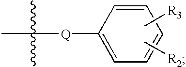
- the present invention relates to an organic light emitting diode device comprising: (a) a cathode; (b) an anode; and (c) at least two organic layers between the anode and the cathode, wherein the at least two organic layers comprise a first organic layer formed from at least one electron-injection/electron-transport material and a second organic layer formed from at least one hole-injection/hole-transport material, wherein the electron-injection/electron-transport material is adjacent to the cathode and the hole-injection/hole-transport material is adjacent to the anode, the at least one hole-injection/hole-transport material comprising a compound of formula 1:
- R 1 is selected from the group consisting of biphenyl, naphthyl, phenyl and
- Q is selected from the group consisting of a bond, C 1 -C 4 alkyl, —C(O)—, —S(O)—, —O—Si—O—, —O—Ge—O—, —O—,
- R 2 and R 3 are each independently selected from the group consisting of aryl, F, Cl, —CF 3 , saturated alkyl of up to 10 carbon atoms, SO 2 R 6, Si(R 6 ) 3 , and OR 6 , or R 2 and R 3 taken together form a heterocyclic ring of up to 8 atoms, wherein one of the 8 atoms is nitrogen and another of the 8 atoms is either nitrogen or oxygen, or R 2 and R 3 taken together with the phenyl group to which they are attached form a fused polycyclic aromatic system, wherein the fused polycyclic aromatic system comprises up to 16 carbon atoms;
- R 4 and R 5 are each independently selected from the group consisting of:
- R 4 and R 5 taken together with the nitrogen to which they are attached are selected from the group consisting of:
- R 6 is C 1 -C 4 straight or branched saturated alkyl
- R 7 and R 8 are each independently selected from the group consisting of —OR 9 , C 1 -C 4 alkyl, aryl, —SCH 3 , —CF 3 , —Cl, —Br, —NO 2 , and —COOR 9 ;
- R 9 is selected from the group consisting Of C 1 -C 6 alkyl and aryl.
- one of the bottom electrode and the top electrode is a cathode and the other is an anode.
- the present invention relates to an organic light emitting diode device comprising: (a) a cathode; (b) an anode; (c) a layer formed from at least one electron-injection/electron-transport material that is adjacent to the cathode; (d) a hole-injection layer that is adjacent to the anode; and (e) at least one hole-transport layer that is adjacent to the hole-injection layer, wherein at least one of the hole-injection and hole-transport layers comprises a compound of formula 1, wherein one of the bottom electrode and the top electrode is a cathode and the other is an anode.
- the present invention relates to an organic light-emitting diode device that emits green light, comprising: (a) a bottom electrode that is an anode comprising indium tin oxide; (b) a hole-injection layer adjacent to the anode comprising bis(N,N′-1-naphthyl-phenyl-amino-biphenyl)-biphenyl amine (BPA-DNPB); (c) a hole-transport layer adjacent to the hole-injection layer comprising bis(carbazol-N-biphenyl)-biphenyl amine (BPA-BCA); (d) an emitter layer adjacent to the hole-transport layer comprising tris(hydroxyquinoline) aluminum (ALQ) and a compound selected from the group consisting of Coumarin 6, Coumarin 485, Coumarin, 487, Coumarin 490, Coumarin 498, Coumarin 500, Coumarin 503, Coumarin 504, Coumarin 504T, Coumarin 510, Coumarin 515,
- the present invention relates to an organic light-emitting diode device that emits white or blue light, comprising: (a) a bottom electrode that is an anode comprising indium tin oxide; (b) a hole-injection layer adjacent to the anode comprising BPA-DNPB; (c) a hole-transport layer adjacent to the hole-injection layer comprising BPA-BCA; (d) an emitter layer adjacent to the hole-transport layer comprising DCJTB, IDE-120 and IDE-102; (e) an electron-transport layer adjacent to the emitter layer comprising ALQ; and (f) a top electrode that is a cathode comprising lithium fluoride and aluminum.
- the present invention relates to a microdisplay device, comprising: (a) at least one bottom electrode that is an anode; (b) at least one top electrode that is a cathode; and (c) at least two organic layers between the at least one bottom electrode and the at least one top electrode, wherein the at least two organic layers comprise a first organic layer formed from at least one electron-injection/electron-transport material that is adjacent to the at least one cathode and a second organic layer formed from at least one hole-injection/hole-transport material that is adjacent to the at least one anode, the at least one hole-injection/hole-transport material comprising a compound of formula 1.
- the present invention relates to an organic light emitting diode device comprising: (a) a cathode; (b) an anode; and (c) at least two organic layers between the anode and the cathode, wherein the at least two organic layers comprise a first organic layer formed from at least one electron-injection/electron-transport material and a second organic layer formed from at least one hole-injection/hole-transport material, wherein the electron-injection/electron-transport material is adjacent to the cathode and the hole-injection/hole-transport material is adjacent to the anode, the at least one hole-injection/hole-transport material comprising a compound of formula 1, wherein R 1 is selected from the group consisting of biphenyl, naphthyl, and phenyl, and wherein one of the bottom electrode and the top electrode is a cathode and the other is an anode.
- the present invention relates to an organic light emitting diode device comprising: (a) a cathode; (b) an anode; and (c) at least two organic layers between the anode and the cathode, wherein the at least two organic layers comprise a first organic layer formed from at least one electron-injection/electron-transport material and a second organic layer formed from at least one hole-injection/hole-transport material, wherein the electron-injection/electron-transport material is adjacent to the cathode and the hole-injection/hole-transport material is adjacent to the anode, the at least one hole-injection/hole-transport material comprising a compound of formula 1, wherein R 1 is selected from the group consisting of biphenyl, naphthyl, phenyl and
- Q is a bond
- one of the bottom electrode and the top electrode is a cathode and the other is an anode
- the present invention relates to an organic light emitting diode device comprising: (a) a cathode; (b) an anode; and (c) at least two organic layers between the anode and the cathode, wherein the at least two organic layers comprise a first organic layer formed from at least one electron-injection/electron-transport material and a second organic layer formed from at least one hole-injection/hole-transport material, wherein the electron-injection/electron-transport material is adjacent to the cathode and the hole-injection/hole-transport material is adjacent to the anode, the at least one hole-injection/hole-transport material comprising a compound of formula 1, wherein R 2 and R 3 are each aryl, and wherein one of the bottom electrode and the top electrode is a cathode and the other is an anode.
- the present invention relates to an organic light emitting diode device comprising: (a) a cathode; (b) an anode; and (c) at least two organic layers between the anode and the cathode, wherein the at least two organic layers comprise a first organic layer formed from at least one electron-injection/electron-transport material and a second organic layer formed from at least one hole-injection/hole-transport material, wherein the electron-injection/electron-transport material is adjacent to the cathode and the hole-injection/hole-transport material is adjacent to the anode, the at least one hole-injection/hole-transport material comprising a compound of formula 1, wherein R 1 is
- R 2 and R 3 are each C 1 -C 4 straight or branched chain alkyl, and wherein one of the bottom electrode and the top electrode is a cathode and the other is an anode.
- the present invention relates to an organic light emitting diode device comprising: (a) a cathode; (b) an anode; and (c) at least two organic layers between the anode and the cathode, wherein the at least two organic layers comprise a first organic layer formed from at least one electron-injection/electron-transport material and a second organic layer formed from at least one hole-injection/hole-transport material, wherein the electron-injection/electron-transport material is adjacent to the cathode and the hole-injection/hole-transport material is adjacent to the anode, the at least one hole-injection/hole-transport material comprising a compound of formula 1, wherein R 4 and R 5 are taken together with the nitrogen to which they are attached are selected from the group consisting of:
- one of the bottom electrode and the top electrode is a cathode and the other is an anode.
- the present invention relates to an organic light emitting diode device comprising: (a) a cathode; (b) an anode; and (c) at least two organic layers between the anode and the cathode, wherein the at least two organic layers comprise a first organic layer formed from at least one electron-injection/electron-transport material and a second organic layer formed from at least one hole-injection/hole-transport material, wherein the electron-injection/electron-transport material is adjacent to the cathode and the hole-injection/hole-transport material is adjacent to the anode, the at least one hole-injection/hole-transport material comprising a compound of formula 1, wherein R 4 and R 5 are taken together with the nitrogen to which they are attached so as to form a heterocycle selected from the group consisting of:
- one of the bottom electrode and the top electrode is a cathode and the other is an anode.
- the present invention relates to an organic light emitting diode device comprising: (a) a cathode; (b) an anode; and (c) at least two organic layers between the anode and the cathode, wherein the at least two organic layers comprise a first organic layer formed from at least one electron-injection/electron-transport material and a second organic layer formed from at least one hole-injection/hole-transport material, wherein the electron-injection/electron-transport material is adjacent to the cathode and the hole-injection/hole-transport material is adjacent to the anode, the at least one hole-injection/hole-transport material comprising a compound of formula 1, wherein R 4 and R 5 are each independently selected from the group consisting of phenyl, naphthyl, biphenyl, anthracenyl and fluorenyl, and wherein one of the bottom electrode and the top electrode is a cathode and the other is an anode.
- FIG. 1 shows an OLED stack.
- FIG. 2 shows an OLED stack comprising a bottom anode and a top cathode on a substrate.
- FIG. 3 shows an OLED stack comprising a bottom cathode and a top anode on a substrate.
- FIG. 4 shows a preferred OLED stack of the present invention.
- OLEDs can be fabricated by any method known to those skilled in the art. In one embodiment, OLEDs are formed by vapor deposition of each layer. In a preferred embodiment, OLEDs are formed by thermal vacuum vapor deposition.
- Bottom electrode means an electrode that is deposited directly onto the substrate.
- Top electrode means an electrode that is deposited at the end of the OLED that is distal to the substrate.
- Hole-injection layer is a layer into which holes are injected from an anode when a voltage is applied across an OLED.
- Hole-transport layer is a layer having high hole mobility and high affinity for holes that is between the anode and the emitter layer. It will be evident to those of skill in the art that the hole-injection layer and the hole-transport layer can be a single layer, or they can be distinct layers comprising different chemical compounds. A compound of formula I is useful both in both hole-injection and hole-transport layers.
- Electrode-injection layer is a layer into which electrons are injected from a cathode when a voltage is applied across an OLED.
- Electrode-transport layer is a layer having high electron mobility and high affinity for electrons that is between the cathode and the emitter layer. It will be evident to those of skill in the art that the electron-injection layer and the electron-transport layer can be a single layer, or they can be distinct layers comprising different chemical compounds.
- an OLED comprises a bottom electrode 102 , which is either an anode or a cathode, a top electrode 101 , which is a cathode if the bottom electrode is an anode and which is an anode if the bottom electrode is a cathode, and an electroluminescent medium having at least two layers 103 , 104 , one comprising at least one hole-injection/hole-transport material that is adjacent to the anode and the other comprising at least one electron-injection/electron-transport layer that is adjacent to the cathode.
- the top electrode is the cathode 201 and the bottom electrode, which is deposited directly onto the substrate 205 , is the anode 202 .
- the cathode and the anode are an electron-injection/electron-transport layer 203 adjacent to the cathode 201 and a hole-injection/hole-transport layer 204 adjacent to the anode 202 .
- the top electrode is the anode 202 and the bottom electrode, which is deposited directly onto the substrate 205 , is the cathode 201 .
- the cathode and the anode are a hole-injection/hole-transport layer 204 adjacent to the anode 202 and an electron-injection/electron-transport layer 203 adjacent to the cathode 201 .
- the top electrode is the cathode 201 and the bottom electrode, which is deposited directly onto the substrate 205 , is the anode 202 .
- the OLED further comprises an electron-transport layer 403 adjacent to the cathode 201 , a hole-injection/hole-transport layer comprising a hole-injection layer 404 adjacent to the anode 202 and at least one hole-transport layer 407 adjacent to the hole-injection layer 404 . Between the electron-transport layer 403 and the hole-transport layer 407 , the OLED further comprises an emitter layer 406 wherein holes and electrons recombine to produce light.
- the OLED comprises a hole-injection layer adjacent to the anode and at least two hole-transport layers, a first hole-transport layer adjacent to the hole-injection layer and a second hole-transport layer adjacent to the first hole-transport layer.
- the hole-injection layer and the at least two hole-transport layers are deposited separately. In another embodiment, at least two of the layers are inter-deposited.
- the OLED comprises an electron-injection layer and at least one electron-transport layer.
- the electroluminescent medium comprises a hole-injection/hole-transport layer adjacent to the anode, an electron-injection/electron-transport layer adjacent to the cathode, and an emitter layer between the hole-injection/hole-transport layer and the electron-injection/electron-transport layer.
- the OLED can further comprise an additional layer adjacent to the top electrode.
- the layer comprises indium tin oxide.
- a typical OLED is formed by starting with a semi-transparent bottom electrode deposited on a glass substrate.
- the electrode is an anode.
- the electrode is a cathode.
- the top electrode is semi-transparent.
- An anode is typically about 800 ⁇ thick and can have one layer comprising a metal having a high work function, a metal oxide and mixtures thereof.
- the anode comprises a material selected from the group consisting of a conducting or semiconducting metal oxide or mixed metal oxide such as indium zinc tin oxide, indium zinc oxide, ruthenium dioxide, molybdenum oxide, nickel oxide or indium tin oxide, a metal having a high work function, such as gold or platinum, and a mixture of a metal oxide and a metal having a high work function.
- the anode further comprises a thin layer (approximately 5-15 ⁇ thick) of dielectric material between the anode and the first hole-injection/hole-transport layer.
- the anode comprises a thin layer of an organic conducting material adjacent to the hole-injection/hole-transport layer.
- organic conducting materials include, but are not limited to, polyaniline, PEDOT-PSS, and a conducting or semi-conducting organic salt thereof.
- a semi-transparent cathode is typically between 70 and 150 ⁇ thick.
- the cathode comprises a single layer of one or more metals, at least one of which has a low work function.
- metals include, but are not limited to, lithium, aluminum, magnesium, calcium, samarium, cesium and mixtures thereof.
- the low work function metal is mixed with a binder metal, such as silver or indium.
- the cathode further comprises a layer of dielectric material adjacent to the electron-injection/electron-transport layer, the dielectric material including, but not limited to, lithium fluoride, cesium fluoride, lithium chloride and cesium chloride.
- the dielectric material is lithium fluoride or cesium fluoride.
- the cathode comprises either aluminum and lithium fluoride, a mixture of magnesium and silver, or a mixture of lithium and aluminum.
- the cathode comprises magnesium, silver and lithium fluoride.
- the hole-injection/hole-transport layer is about 750 ⁇ thick.
- the hole-injection/hole-transport material comprises a compound of formula 1.
- the hole-injection/hole-transport layer comprises a hole-injection layer comprising BPA-DNPB and a hole-transport layer comprising BPA-BCA.
- an OLED comprises an emitter layer between the electron-injection/electron-transport layer and the hole-injection/hole-transport layer in which electrons from the electron-injection/electron-transport layer and holes from the hole-injecting/hole-transport layer recombine.
- OLEDs emit visible light of different colors.
- Emitter layers typically comprise at least one host compound, either alone or together with at least one dopant compound. Examples of host compounds include, but are not limited to, ALQ, IDE-120 and IDE-140 (Idemitsu Kosan Co., Ltd., Tokyo, Japan).
- Examples of dopant compounds include, but are not limited to, Coumarin 6, Coumarin 485, Coumarin, 487, Coumarin 490, Coumarin 498, Coumarin 500, Coumarin 503, Coumarin 504, Coumarin 504T, Coumarin 510, Coumarin 515, Coumarin 519, Coumarin 521, Coumarin 521T, Coumarin 522B, Coumarin 523, Coumarin 525, Coumarin 535, Coumarin 540A, Coumarin 545, quinacridone derivatives such as diethyl pentyl quinacridone and dimethyl quinacridone, distyrylamine derivatives, such as IDE-102, IDE-105 (Idemitsu Kosan Co., Ltd., Tokyo, Japan), rubrene, DCJTB, pyrromethane 546, and mixtures thereof.
- the structure of DCJTB is shown below:
- An emitter layer may be between 200-400 ⁇ thick.
- the electron-injection/electron-transport layer is typically about 350 ⁇ thick and comprises a compound such as ALQ, or a suitable oxadiazole derivative. In a preferred embodiment, the electron-injection/electron-transport layer is ALQ.
- an OLED of the present invention comprises a 750 ⁇ thick hole-injection/hole-transport layer of bis(N,N′-1-naphthyl-phenyl-amino-biphenyl)-1-naphthyl amine (NA-DNPB), a 750 ⁇ thick emitter/electron transport layer of ALQ, and either Mg:Ag or LiF/Al cathode.
- an OLED of the present invention comprises a 550 ⁇ thick hole-injection layer of BPA-DNPB, a 200 ⁇ thick hole-transport layer of BPA-BCA, a 350 ⁇ thick emitter layer of ALQ doped with 2.5% of coumarin 6, a 300 ⁇ thick electron transport layer of ALQ, and a cathode that is either Mg:Ag or aluminum on lithium fluoride.
- an OLED of the present invention is a down-emitter that emits green light and comprises an anode comprising indium tin oxide, a hole-injection layer adjacent to the anode comprising BPA-DNPB, a hole-transport layer adjacent to the hole-injection layer comprising BPA-BCA, an emitter layer adjacent to the hole-transport layer comprising ALQ and a compound selected from the group consisting of Coumarin 6, Coumarin 485, Coumarin, 487, Coumarin 490, Coumarin 498, Coumarin 500, Coumarin 503, Coumarin 504, Coumarin 504T, Coumarin 510, Coumarin 515, Coumarin 519, Coumarin 521, Coumarin 521T, Coumarin 522B, Coumarin 523, Coumarin 525, Coumarin 535, Coumarin 540A, Coumarin 545, and mixtures thereof, an electron-transport layer adjacent to the emitter layer comprising ALQ, and a cathode comprising either lithium fluoride and aluminum or magnesium and silver.
- an OLED of the present invention is an up-emitter that emits green light and comprises an anode comprising molybdenum oxide, a hole-injection layer adjacent to the anode comprising BPA-DNPB, a hole-transport layer adjacent to the hole-injection layer comprising BPA-BCA, an emitter layer adjacent to the hole-transport layer comprising ALQ and a compound selected from the group consisting of Coumarin 6, Coumarin 485, Coumarin, 487, Coumarin 490, Coumarin 498, Coumarin 500, Coumarin 503, Coumarin 504, Coumarin 504T, Coumarin 510, Coumarin 515, Coumarin 519, Coumarin 521, Coumarin 521T, Coumarin 522B, Coumarin 523, Coumarin 525, Coumarin 535, Coumarin 540A, Coumarin 545, and mixtures thereof, an electron-transport layer adjacent to the emitter layer comprising ALQ, and a cathode comprising lithium fluoride, magnesium and silver.
- an OLED of the present invention emits white or blue light and comprises an anode comprising indium tin oxide, a hole-injection layer adjacent to the anode comprising BPA-DNPB, a hole-transport layer adjacent to the hole-injection layer comprising BPA-B CA, an emitter layer adjacent to the hole-transport layer comprising DCJTB, IDE-102 and IDE-120, an electron-transport layer adjacent to the emitter layer comprising ALQ, and a cathode comprising lithium fluoride and aluminum.
- the OLED display device is a microdisplay.
- a microdisplay is a display device that is not viewable by the unaided eye, and therefore requires the use of an optic.
- the sub-pixel size of a microdisplay device is less than about 15 microns, more preferably less than about 5 microns, and most preferably between about 2 microns and about 3 microns.
- the multi-layered OLED devices of the invention allow for a “staircase” change in the energy difference of electrons and holes as they travel from the electrodes through each layer toward the emitter layer, where they recombine to emit light.
- the anode and cathode of an OLED have an energy difference of about 1.6-1.8 eV.
- a typical band gap of electrons and holes in the emitter layer is about 2.7 eV-2.9 eV, so that radiation emission resulting from recombination is in the visible light region (1.75 to 3 eV).
- the increase in energy difference of holes and electrons from the anode and cathode to the emitter layer is accomplished incrementally as the electrons and holes travel through the layers between the electrodes and the emitter layer.
- the energy difference is increased in increments of about 0.2-0.3 eV per layer to achieve the resulting band gap of 2.7 eV-2.9 eV in the emitter layer.
- a staircase change in energy provides for a lower operating voltage and better efficiency of operation of the OLED device, resulting in a higher quantum yield of luminescence for a given current density.
- the present invention relates to OLEDs having incorporated in the electroluminescent medium organic compounds with variable ionization potentials (IP) and electron affinities (EA) and high glass transition temperatures. Specifically, the present invention relates to OLEDs having hole-injection and hole-transport layers with variable IP and high glass transition temperatures. In particular, the present invention relates to OLEDs having hole-injection and hole-transport layers comprising a compound of formula 1:
- R 1 is selected from the group consisting of biphenyl, naphthyl, phenyl and
- Q is selected from the group consisting of a bond, C 1 -C 4 alkyl, —C(O)—, —S(O)—, —O—Si—O—, —O—Ge—O—, —O—,
- R 2 and R 3 are each independently selected from the group consisting of aryl, F, Cl, —CF 3 , saturated alkyl of up to 10 carbon atoms, preferably of between 1 and 4 carbon atoms, SO 2 R 6 , Si(R 6 ) 3 , and OR 6 , or R 2 and R 3 taken together form a heterocyclic ring of up to 8 atoms, wherein one of the 8 atoms is nitrogen and another of the 8 atoms is either nitrogen or oxygen, or R 2 and R 3 taken together with the phenyl group to which they are attached form a fused polycyclic aromatic system, wherein the fused polycyclic aromatic system comprises up to 16 carbon atoms;
- R 4 and R 5 are each independently selected from the group consisting of:
- R 4 and R 5 taken together with the nitrogen to which they are attached are selected from the group consisting of:
- R 6 is C 1 -C 4 straight or branched saturated alkyl
- R 7 and R 8 are each independently selected from the group consisting of —OR 9 , C 1 -C 4 alkyl, aryl, —SCH 3 , —CF 3 , —Cl, —Br, —NO 2 , and —COOR 9 ; and
- R 9 is selected from the group consisting of C 1 -C 6 alkyl and aryl.
- Additional compounds for this embodiment include compounds of formula 1, wherein R 4 and R 5 are each independently selected from the group consisting of:
- Such OLEDs incorporating organic compounds with variable IP and high glass transition temperatures in the hole-injection and hole-transport layers are longer-lived and can withstand higher temperatures than OLEDs that incorporate traditional triarylamines in those layers.
- the variable IP of these materials also permits staircase tuning of the hole energies to increase the quantum efficiency of the OLEDs.
- Hole-injection and hole-transport layers comprising a compound of formula 1 typically have glass transition temperatures in the range of 130-180° C. Therefore, the OLEDs of the present invention can be operated at higher current densities, which results in increased brightness, without changing the morphology of the hole-injection and hole-transport layers and degrading the device.
- Hole-injection and hole-transport compounds useful in OLEDs of the present invention can be made as shown in Scheme I.
- DPPF diphenylphosphino ferrocene
- Pd 2 (dba) 3 tris(dibenzylideneacetone) dipalladium
- the reaction mixture is then heated to about 95° C. for about 20 hours.
- the thermal properties and glass transition temperatures of compounds of formula 1 are determined using differential scanning calorimetry (DSC) and thermo gravimetric analysis (TGA).
- Silica gel having average particle size of 230-400 mesh from Whatman was used in a 20 cm column for purification. Compounds were eluted using 5% CH 2 Cl 2 in hexane as the mobile phase.
- Sublimation was performed using a train sublimation apparatus designed in the laboratory at a pressure of 1.0 ⁇ 10 ⁇ 6 torr and at temperature of 350 ° C.
- Mass spectroscopy was performed on a SFNNIGAN 4500 instrument from Sfnnigan Corporation using direct ionization with methane as the gas at a pressure of 0.4 millitorr.
- TGA was performed on a TGA-50 instrument from Shimadzu.
- DSC was performed using a DSC-50 instrument from Shimadzu.
- BPA-BPBBr biphenylamino-bis-biphenyl bromide
- NA-BPBBr 1-naphthyl-amino-bis-biphenyl bromide
- NA-DNPB (8) was isolated by silica gel chromatography (see Materials, Example 1, above). 1.5 g of crude product was obtained (85% yield). NA-DNPB (8) was further purified by sublimation (see Materials, Example 1, above). Mass spectroscopic analysis (see Materials, Example 1, above) confirmed the formation of NA-DNPB (8).
- the glass transition temperature (T g ) was determined by DSC (see Materials, Example 1, above) to be about 147° C.
- NA-BPBBr was synthesized as described above in Example 2.
- NA-BCA (9) was isolated by silica gel chromatography (see Materials, Example 1, above). 1.20 g of crude product was obtained (85% yield). NA-BCA (9) was further purified by sublimation (see Materials, Example 1, above). Mass spectroscopic analysis (see Materials, Example 1, above) confirmed the formation of NA-BCA (9).
- a 750 ⁇ thick hole-injection/hole-transport layer of BPA-BCA was thermally evaporated on pre-cleaned indium tin oxide (ITO) substrate in high vacuum (10 ⁇ 6 -10 ⁇ 7 torr) at room temperature. This was followed by evaporation of a 750 ⁇ thick emitter/electron transport layer of ALQ.
- a cathode comprising a 7.5 ⁇ layer of LiF followed by a 500 ⁇ layer of Al was then deposited. The resulting OLED demonstrated diode behavior and emitted green light when direct voltage was applied.
- the OLED demonstrated quantum efficiency of 5.2 cd/A and 1.6% ph/e, a low driving voltage (6.8 Volts) at a current density of 20 mA/cm 2 , and a brightness level of 590 cd/m 2 for green emission.
- a 750 ⁇ thick hole-injection/hole-transport layer of NA-DNPB was thermally evaporated on pre-cleaned indium tin oxide (ITO) substrate that has been ashed in oxygen plasma (400 W power, 300 millitorr pressure, oxygen flow 50 cc/min) for one minute (see Example 4, above). This was followed by evaporation of a 750 ⁇ thick emitter/electron transport layer of ALQ and a either a Mg:Ag or LiF/A1 cathode (see Example 4, above). The resulting OLED demonstrated diode behavior and emitted green light when direct voltage was applied.
- ITO indium tin oxide
- the OLED demonstrated quantum efficiency of 2.95 cd/A and 0.91% ph/e, a low driving voltage (7.4 Volts) at a current density of 20 InA/cm 2 , and a brightness level of 1053 cd/m 2 for green emission.
- a 550 ⁇ thick hole-injection layer of BPA-DNPB was thermally evaporated on pre-cleaned indium tin oxide (ITO) substrate in high vacuum (see Example 5, above). This was followed by evaporation of a 200 ⁇ thick hole-transport layer of BPA-BCA, evaporation of a 350 ⁇ thick emitter layer of ALQ doped with 2.5% of coumarin 6 (see Example 4, above), and evaporation of a 300 ⁇ thick electron transport layer of ALQ, and a LiF/A1 cathode (see Example 4, above). The resulting OLED demonstrated diode behavior and emitted green light when direct voltage was applied.
- ITO indium tin oxide
- the OLED demonstrated quantum efficiency of 14.3 cd/A and 4.0% ph/e, a low driving voltage (7.0 Volts) at a current density of 20 mA/cm 2 , and a brightness level of 2,900 cd/m 2 for green emission.
Abstract
Description


Claims (79)


Priority Applications (1)
| Application Number | Priority Date | Filing Date | Title |
|---|---|---|---|
| US09/894,502 US6657224B2 (en) | 2001-06-28 | 2001-06-28 | Organic light emitting diode devices using thermostable hole-injection and hole-transport compounds |
Applications Claiming Priority (1)
| Application Number | Priority Date | Filing Date | Title |
|---|---|---|---|
| US09/894,502 US6657224B2 (en) | 2001-06-28 | 2001-06-28 | Organic light emitting diode devices using thermostable hole-injection and hole-transport compounds |
Publications (2)
| Publication Number | Publication Date |
|---|---|
| US20030030059A1 US20030030059A1 (en) | 2003-02-13 |
| US6657224B2 true US6657224B2 (en) | 2003-12-02 |
Family
ID=25403165
Family Applications (1)
| Application Number | Title | Priority Date | Filing Date |
|---|---|---|---|
| US09/894,502 Expired - Lifetime US6657224B2 (en) | 2001-06-28 | 2001-06-28 | Organic light emitting diode devices using thermostable hole-injection and hole-transport compounds |
Country Status (1)
| Country | Link |
|---|---|
| US (1) | US6657224B2 (en) |
Cited By (9)
| Publication number | Priority date | Publication date | Assignee | Title |
|---|---|---|---|---|
| US20020021088A1 (en) * | 1998-05-18 | 2002-02-21 | Howard Webster E. | Organic light emitting diode devices with improved anode stability |
| US20050196960A1 (en) * | 2002-10-17 | 2005-09-08 | Kyeong-Mo Koo | Method of forming metal silicide film and method of manufacturing semiconductor device having metal silicide film |
| US20050202280A1 (en) * | 2002-06-01 | 2005-09-15 | Su-Bin Song | Organic electroluminescence device |
| US20070003785A1 (en) * | 2005-06-30 | 2007-01-04 | Eastman Kodak Company | Electroluminescent devices containing benzidine derivatives |
| US20070262302A1 (en) * | 2006-05-15 | 2007-11-15 | Amane Mochizuki | Light emitting devices and compositions |
| US20090066234A1 (en) * | 2007-07-05 | 2009-03-12 | Hyun Sik Chae | Light emitting devices and compositions |
| US20100094056A1 (en) * | 2006-12-13 | 2010-04-15 | Rene Csuk | Arylamine-substituted divinyl fluorenes and their use for electrophotographic applications, and for oleds (organic light emitting devices) |
| US20110193075A1 (en) * | 2008-10-13 | 2011-08-11 | Amane Mochizuki | Printable light-emitting compositions |
| US8597803B2 (en) | 2007-11-15 | 2013-12-03 | Nitto Denko Corporation | Light emitting devices and compositions |
Families Citing this family (11)
| Publication number | Priority date | Publication date | Assignee | Title |
|---|---|---|---|---|
| US20030153141A1 (en) * | 2001-12-20 | 2003-08-14 | Carter Susan A. | Screen printable electrode for light emitting polymer device |
| US20030230980A1 (en) * | 2002-06-18 | 2003-12-18 | Forrest Stephen R | Very low voltage, high efficiency phosphorescent oled in a p-i-n structure |
| TW595251B (en) * | 2002-12-09 | 2004-06-21 | Univ Nat Cheng Kung | Method for manufacturing organic light-emitting diodes |
| US7732808B2 (en) * | 2003-09-26 | 2010-06-08 | Semiconductor Energy Laboratory Co., Ltd | Light-emitting device and method for manufacturing the same |
| CN1738069A (en) * | 2004-08-17 | 2006-02-22 | 国际商业机器公司 | Method for manufacturing electronic device having an electrode with enhanced injection properties and said electronic device |
| US8420227B2 (en) * | 2005-03-23 | 2013-04-16 | Semiconductor Energy Laboratory Co., Ltd. | Composite material, light emitting element and light emitting device |
| US20070215889A1 (en) * | 2006-03-20 | 2007-09-20 | Semiconductor Energy Laboratory Co., Ltd. | Aromatic amine compound, and light-emitting element, light-emitting device, and electronic appliance using the aromatic amine compound |
| KR101640307B1 (en) * | 2013-08-19 | 2016-07-15 | 주식회사 엘지화학 | Aromatic compounds and organic electronic device comprising the same |
| US10319912B2 (en) * | 2015-01-29 | 2019-06-11 | Samsung Electronics Co., Ltd. | Charge-transporting material and organic light-emitting device including the same |
| CN106654047B (en) * | 2016-12-22 | 2019-02-01 | 武汉华星光电技术有限公司 | OLED display panel and preparation method thereof |
| CN112510161B (en) * | 2020-12-02 | 2022-02-11 | 吉林大学 | Color-adjustable organic electroluminescent device and preparation method thereof |
Citations (10)
| Publication number | Priority date | Publication date | Assignee | Title |
|---|---|---|---|---|
| JPH04320485A (en) * | 1991-04-19 | 1992-11-11 | Mitsubishi Kasei Corp | Organic electroluminescent device |
| US5536949A (en) * | 1992-08-28 | 1996-07-16 | Idemistu Kosan Co., Ltd. | Charge injection auxiliary material and organic electroluminescence device containing the same |
| EP0848579A2 (en) | 1996-12-16 | 1998-06-17 | Toyo Ink Manufacturing Co., Ltd. | Material for organoelectroluminescence device and organelectroluminescence device using the material |
| WO1999020596A1 (en) | 1997-10-20 | 1999-04-29 | Chisso Corporation | Amine derivatives and organic electroluminescent device made by using the same |
| EP0969532A2 (en) | 1998-07-04 | 2000-01-05 | Bayer Aktiengesellschaft | Electroluminescent devices using metal complexes of azomethine |
| EP0973210A2 (en) | 1998-07-16 | 2000-01-19 | Sumitomo Electric Industries, Ltd. | Triphenylamine derivative and organic electroluminescence device comprising the same |
| US6114055A (en) * | 1998-06-01 | 2000-09-05 | Motorola, Inc. | Organic electroluminescent device with continuous organic medium containing rubrene |
| US6194089B1 (en) * | 1998-06-11 | 2001-02-27 | Motorola, Inc. | Organic electroluminescent device with improved reliability |
| US20020034655A1 (en) * | 2000-04-28 | 2002-03-21 | Teruichi Watanabe | Organic electroluminescence element |
| US6406804B1 (en) * | 1998-04-09 | 2002-06-18 | Idemitsu Kosan Co., Ltd. | Organic electroluminescent device |
-
2001
- 2001-06-28 US US09/894,502 patent/US6657224B2/en not_active Expired - Lifetime
Patent Citations (10)
| Publication number | Priority date | Publication date | Assignee | Title |
|---|---|---|---|---|
| JPH04320485A (en) * | 1991-04-19 | 1992-11-11 | Mitsubishi Kasei Corp | Organic electroluminescent device |
| US5536949A (en) * | 1992-08-28 | 1996-07-16 | Idemistu Kosan Co., Ltd. | Charge injection auxiliary material and organic electroluminescence device containing the same |
| EP0848579A2 (en) | 1996-12-16 | 1998-06-17 | Toyo Ink Manufacturing Co., Ltd. | Material for organoelectroluminescence device and organelectroluminescence device using the material |
| WO1999020596A1 (en) | 1997-10-20 | 1999-04-29 | Chisso Corporation | Amine derivatives and organic electroluminescent device made by using the same |
| US6406804B1 (en) * | 1998-04-09 | 2002-06-18 | Idemitsu Kosan Co., Ltd. | Organic electroluminescent device |
| US6114055A (en) * | 1998-06-01 | 2000-09-05 | Motorola, Inc. | Organic electroluminescent device with continuous organic medium containing rubrene |
| US6194089B1 (en) * | 1998-06-11 | 2001-02-27 | Motorola, Inc. | Organic electroluminescent device with improved reliability |
| EP0969532A2 (en) | 1998-07-04 | 2000-01-05 | Bayer Aktiengesellschaft | Electroluminescent devices using metal complexes of azomethine |
| EP0973210A2 (en) | 1998-07-16 | 2000-01-19 | Sumitomo Electric Industries, Ltd. | Triphenylamine derivative and organic electroluminescence device comprising the same |
| US20020034655A1 (en) * | 2000-04-28 | 2002-03-21 | Teruichi Watanabe | Organic electroluminescence element |
Cited By (16)
| Publication number | Priority date | Publication date | Assignee | Title |
|---|---|---|---|---|
| US20020021088A1 (en) * | 1998-05-18 | 2002-02-21 | Howard Webster E. | Organic light emitting diode devices with improved anode stability |
| US6885147B2 (en) * | 1998-05-18 | 2005-04-26 | Emagin Corporation | Organic light emitting diode devices with improved anode stability |
| US20050202280A1 (en) * | 2002-06-01 | 2005-09-15 | Su-Bin Song | Organic electroluminescence device |
| US7166370B2 (en) * | 2002-06-01 | 2007-01-23 | Samsung Sdi Co., Ltd. | Organic electroluminescence device |
| US20050196960A1 (en) * | 2002-10-17 | 2005-09-08 | Kyeong-Mo Koo | Method of forming metal silicide film and method of manufacturing semiconductor device having metal silicide film |
| US20070003785A1 (en) * | 2005-06-30 | 2007-01-04 | Eastman Kodak Company | Electroluminescent devices containing benzidine derivatives |
| US20070262302A1 (en) * | 2006-05-15 | 2007-11-15 | Amane Mochizuki | Light emitting devices and compositions |
| US7993747B2 (en) * | 2006-05-15 | 2011-08-09 | Nitto Denko Corporation | Light emitting devices and compositions comprising lumophore-functionalized nanoparticles |
| US20100094056A1 (en) * | 2006-12-13 | 2010-04-15 | Rene Csuk | Arylamine-substituted divinyl fluorenes and their use for electrophotographic applications, and for oleds (organic light emitting devices) |
| US8629300B2 (en) | 2006-12-13 | 2014-01-14 | Sensient Imaging Technologies Gmbh | Arylamine-substituted divinyl fluorenes and their use for electrophotographic applications, and for OLEDs (organic light emitting devices) |
| US20090066234A1 (en) * | 2007-07-05 | 2009-03-12 | Hyun Sik Chae | Light emitting devices and compositions |
| US20120305895A1 (en) * | 2007-07-05 | 2012-12-06 | Hyun Sik Chae | Light emitting devices and compositions |
| US8609258B2 (en) * | 2007-07-05 | 2013-12-17 | Nitto Denko Corporation | Light emitting devices and compositions |
| US8597803B2 (en) | 2007-11-15 | 2013-12-03 | Nitto Denko Corporation | Light emitting devices and compositions |
| US20110193075A1 (en) * | 2008-10-13 | 2011-08-11 | Amane Mochizuki | Printable light-emitting compositions |
| US8721922B2 (en) | 2008-10-13 | 2014-05-13 | Nitto Denko Corporation | Printable light-emitting compositions |
Also Published As
| Publication number | Publication date |
|---|---|
| US20030030059A1 (en) | 2003-02-13 |
Similar Documents
| Publication | Publication Date | Title |
|---|---|---|
| US6150043A (en) | OLEDs containing thermally stable glassy organic hole transporting materials | |
| US6657224B2 (en) | Organic light emitting diode devices using thermostable hole-injection and hole-transport compounds | |
| KR102213030B1 (en) | Novel boron compounds and Organic light emitting diode including the same | |
| US6387544B1 (en) | OLEDS containing thermally stable glassy organic hole transporting materials | |
| US6646164B2 (en) | Triphenylamine derivative and organic electroluminescence device comprising the same | |
| CN109748898B (en) | Organic electroluminescent compound, preparation method thereof and organic electroluminescent device | |
| US20020057050A1 (en) | Organic light emitting diode devices using aromatic amine compounds with high and tunable glass transition temperatures | |
| KR102169273B1 (en) | Organic electroluminescent compound comprising acridine derivative and organic electroluminescent device comprising same | |
| US6838194B2 (en) | Efficient organic electroluminescent devices with red fluorescent dopants | |
| CN106883205B (en) | Novel compound and organic light-emitting device comprising same | |
| KR101026175B1 (en) | Fluorenecarbazole derivative and organic electroluminescent device comprising same | |
| KR20090114716A (en) | Hole transporting layer material and organic electroluminescent device comprising the same | |
| JP4631259B2 (en) | Organic electroluminescence element and display device | |
| KR100994765B1 (en) | Organic electroluminescent device comprising fluorene-based light emitting material | |
| CN109776334B (en) | Organic electroluminescent compounds, method of manufacturing the same and devices using the same | |
| KR102239994B1 (en) | Novel boron compounds and Organic light emitting diode including the same | |
| CN106573905B (en) | Light-emitting compound and organic light-emitting element comprising same | |
| KR101694496B1 (en) | Dibenzothiophene derivative compound and organic electroluminescent device using the same | |
| KR20100007639A (en) | Novel phenyl-fluorene derivatives and organic electroluminescent device comprising the same | |
| US6649089B2 (en) | Red organic electroluminescent materials | |
| JP2001244076A (en) | Organic elemctroluminescent element manufactured by using acridine derivative compound | |
| JP7215065B2 (en) | Aminocarbazole compound and use thereof | |
| WO2003003482A1 (en) | Organic light emitting diode devices using thermostable hole-injection and hole-transport compounds | |
| JP2014108940A (en) | Indolocarbazole derivative and organic electroluminescence device including the same | |
| US7037600B2 (en) | Red-emitting organic electroluminescent elements |
Legal Events
| Date | Code | Title | Description |
|---|---|---|---|
| AS | Assignment |
Owner name: EMAGIN CORPORATION, NEW YORK Free format text: ASSIGNMENT OF ASSIGNORS INTEREST;ASSIGNORS:SHI, XIAOBO;SOKOLIK, IGOR;REEL/FRAME:011978/0633 Effective date: 20010627 |
|
| AS | Assignment |
Owner name: VERSUS SUPPORT SERVICES INC., NEW YORK Free format text: SECURITY INTEREST;ASSIGNOR:EMAGIN CORPORATION;REEL/FRAME:012454/0893 Effective date: 20011121 |
|
| AS | Assignment |
Owner name: ALLIGATOR HOLDINGS, INC., NEW YORK Free format text: ASSIGNMENT OF SECURITY INTEREST;ASSIGNOR:VERUS SUPPORT SERVICES INC.;REEL/FRAME:012991/0057 Effective date: 20020620 |
|
| AS | Assignment |
Owner name: ALLIGATOR HOLDINGS, INC., NEW YORK Free format text: SECURITY AGREEMENT;ASSIGNOR:EMAGIN CORPORATION;REEL/FRAME:012983/0846 Effective date: 20020620 |
|
| AS | Assignment |
Owner name: ALLIGATOR HOLDINGS, INC., NEW YORK Free format text: SECURITY INTEREST;ASSIGNOR:EMAGIN CORPORATION;REEL/FRAME:014007/0352 Effective date: 20030422 |
|
| STCF | Information on status: patent grant |
Free format text: PATENTED CASE |
|
| AS | Assignment |
Owner name: EMAGIN CORPORATION, NEW YORK Free format text: RELEASE BY SECURED PARTY;ASSIGNOR:ALLIGATOR HOLDINGS, INC.;REEL/FRAME:017858/0054 Effective date: 20060630 |
|
| AS | Assignment |
Owner name: ALEXANDRA GLOBAL MASTER FUND LTD.,NEW YORK Free format text: SECURITY AGREEMENT;ASSIGNOR:EMAGIN CORPORATION;REEL/FRAME:017982/0743 Effective date: 20060721 Owner name: ALEXANDRA GLOBAL MASTER FUND LTD., NEW YORK Free format text: SECURITY AGREEMENT;ASSIGNOR:EMAGIN CORPORATION;REEL/FRAME:017982/0743 Effective date: 20060721 |
|
| FEPP | Fee payment procedure |
Free format text: PAT HOLDER CLAIMS SMALL ENTITY STATUS, ENTITY STATUS SET TO SMALL (ORIGINAL EVENT CODE: LTOS); ENTITY STATUS OF PATENT OWNER: SMALL ENTITY |
|
| FPAY | Fee payment |
Year of fee payment: 4 |
|
| AS | Assignment |
Owner name: MORIAH CAPITAL, L.P., NEW YORK Free format text: SECURITY AGREEMENT;ASSIGNOR:EMAGIN CORPORATION;REEL/FRAME:020098/0610 Effective date: 20070807 Owner name: MORIAH CAPITAL, L.P.,NEW YORK Free format text: SECURITY AGREEMENT;ASSIGNOR:EMAGIN CORPORATION;REEL/FRAME:020098/0610 Effective date: 20070807 |
|
| AS | Assignment |
Owner name: EMAGIN CORPORATION, NEW YORK Free format text: RELEASE BY SECURED PARTY;ASSIGNOR:MORIAH CAPITAL, L.P.;REEL/FRAME:025169/0107 Effective date: 20101018 |
|
| FPAY | Fee payment |
Year of fee payment: 8 |
|
| AS | Assignment |
Owner name: EMAGIN CORPORATION, NEW YORK Free format text: RELEASE OF SECURITY INTEREST;ASSIGNOR:ALEXANDRA GLOBAL MASTER FUND LTD.;REEL/FRAME:033417/0309 Effective date: 20140722 |
|
| FPAY | Fee payment |
Year of fee payment: 12 |