WO2002005971A1 - Organic-inorganic hybrid light emitting devices (hled) - Google Patents

Organic-inorganic hybrid light emitting devices (hled) Download PDF

Info

Publication number
WO2002005971A1
WO2002005971A1 PCT/US2001/041351 US0141351W WO0205971A1 WO 2002005971 A1 WO2002005971 A1 WO 2002005971A1 US 0141351 W US0141351 W US 0141351W WO 0205971 A1 WO0205971 A1 WO 0205971A1
Authority
WO
WIPO (PCT)
Prior art keywords
organic
hled
inorganic
moiety
moieties
Prior art date
Application number
PCT/US2001/041351
Other languages
French (fr)
Inventor
Alan Sellinger
Richard M. Laine
Original Assignee
Canon Kabushiki Kaisha
Priority date (The priority date is an assumption and is not a legal conclusion. Google has not performed a legal analysis and makes no representation as to the accuracy of the date listed.)
Filing date
Publication date
Application filed by Canon Kabushiki Kaisha filed Critical Canon Kabushiki Kaisha
Priority to JP2002511899A priority Critical patent/JP3880518B2/en
Priority to KR10-2003-7000480A priority patent/KR20030043909A/en
Publication of WO2002005971A1 publication Critical patent/WO2002005971A1/en

Links

Classifications

    • HELECTRICITY
    • H10SEMICONDUCTOR DEVICES; ELECTRIC SOLID-STATE DEVICES NOT OTHERWISE PROVIDED FOR
    • H10KORGANIC ELECTRIC SOLID-STATE DEVICES
    • H10K85/00Organic materials used in the body or electrodes of devices covered by this subclass
    • H10K85/10Organic polymers or oligomers
    • H10K85/111Organic polymers or oligomers comprising aromatic, heteroaromatic, or aryl chains, e.g. polyaniline, polyphenylene or polyphenylene vinylene
    • H10K85/115Polyfluorene; Derivatives thereof
    • CCHEMISTRY; METALLURGY
    • C07ORGANIC CHEMISTRY
    • C07FACYCLIC, CARBOCYCLIC OR HETEROCYCLIC COMPOUNDS CONTAINING ELEMENTS OTHER THAN CARBON, HYDROGEN, HALOGEN, OXYGEN, NITROGEN, SULFUR, SELENIUM OR TELLURIUM
    • C07F7/00Compounds containing elements of Groups 4 or 14 of the Periodic System
    • C07F7/02Silicon compounds
    • C07F7/08Compounds having one or more C—Si linkages
    • HELECTRICITY
    • H10SEMICONDUCTOR DEVICES; ELECTRIC SOLID-STATE DEVICES NOT OTHERWISE PROVIDED FOR
    • H10KORGANIC ELECTRIC SOLID-STATE DEVICES
    • H10K85/00Organic materials used in the body or electrodes of devices covered by this subclass
    • H10K85/40Organosilicon compounds, e.g. TIPS pentacene
    • HELECTRICITY
    • H10SEMICONDUCTOR DEVICES; ELECTRIC SOLID-STATE DEVICES NOT OTHERWISE PROVIDED FOR
    • H10KORGANIC ELECTRIC SOLID-STATE DEVICES
    • H10K85/00Organic materials used in the body or electrodes of devices covered by this subclass
    • H10K85/60Organic compounds having low molecular weight
    • H10K85/615Polycyclic condensed aromatic hydrocarbons, e.g. anthracene
    • HELECTRICITY
    • H10SEMICONDUCTOR DEVICES; ELECTRIC SOLID-STATE DEVICES NOT OTHERWISE PROVIDED FOR
    • H10KORGANIC ELECTRIC SOLID-STATE DEVICES
    • H10K85/00Organic materials used in the body or electrodes of devices covered by this subclass
    • H10K85/60Organic compounds having low molecular weight
    • H10K85/631Amine compounds having at least two aryl rest on at least one amine-nitrogen atom, e.g. triphenylamine
    • HELECTRICITY
    • H10SEMICONDUCTOR DEVICES; ELECTRIC SOLID-STATE DEVICES NOT OTHERWISE PROVIDED FOR
    • H10KORGANIC ELECTRIC SOLID-STATE DEVICES
    • H10K85/00Organic materials used in the body or electrodes of devices covered by this subclass
    • H10K85/60Organic compounds having low molecular weight
    • H10K85/649Aromatic compounds comprising a hetero atom
    • H10K85/656Aromatic compounds comprising a hetero atom comprising two or more different heteroatoms per ring
    • H10K85/6565Oxadiazole compounds
    • HELECTRICITY
    • H10SEMICONDUCTOR DEVICES; ELECTRIC SOLID-STATE DEVICES NOT OTHERWISE PROVIDED FOR
    • H10KORGANIC ELECTRIC SOLID-STATE DEVICES
    • H10K50/00Organic light-emitting devices
    • H10K50/10OLEDs or polymer light-emitting diodes [PLED]
    • H10K50/11OLEDs or polymer light-emitting diodes [PLED] characterised by the electroluminescent [EL] layers
    • YGENERAL TAGGING OF NEW TECHNOLOGICAL DEVELOPMENTS; GENERAL TAGGING OF CROSS-SECTIONAL TECHNOLOGIES SPANNING OVER SEVERAL SECTIONS OF THE IPC; TECHNICAL SUBJECTS COVERED BY FORMER USPC CROSS-REFERENCE ART COLLECTIONS [XRACs] AND DIGESTS
    • Y10TECHNICAL SUBJECTS COVERED BY FORMER USPC
    • Y10STECHNICAL SUBJECTS COVERED BY FORMER USPC CROSS-REFERENCE ART COLLECTIONS [XRACs] AND DIGESTS
    • Y10S428/00Stock material or miscellaneous articles
    • Y10S428/917Electroluminescent

Definitions

  • the present invention relates to compositions used to fabricate light emitting devices, more specifically, the present invention is drawn to organic-inorganic hybrid light emitting devices (HLED) fabricating with light emitting compositions in which hole transport, electron transport, and emissive compounds are covalently linked to polyhedral silsesquioxanes.
  • HLED organic-inorganic hybrid light emitting devices
  • OLEDs organic light emitting devices
  • LCD liquid crystal display
  • RGB red, green and blue
  • OLEDs The scientific basis for OLEDs relies on an organic material's ability to emit light when subjected to electrical stimuli.
  • electrons and holes are injected into organic materials from conducting electrodes and diffuse through a thin organic film to form electron-hole pairs or excitons within a highly conjugated organic molecule or polymer layer.
  • the excitons then recombine creating an excited state within the organic molecule.
  • the excited state can then undergo radiative decay emitting a photon.
  • the wavelength of light emitted can be any color and even multicolored, e.g. red, green, blue or combinations thereof. For optimal operation, it is important that the rate at which the holes and electrons diffuse into this emitting layer be similar, and preferably matched.
  • the OLED device 10 was prepared by sandwiching organic hole transport (HT) material 12 and emissive (EM) material 14 between an indium-tin-oxide (ITO) anode 16 and magnesium/silver alloy cathode 18 layers.
  • a conventional electric potential source 20 was connected to the cathode 18 and anode 16.
  • a glass substrate 22 allowed light emission as shown by Arrow 24.
  • the hole transport (HT) and emissive (EM) materials used by Tang and Nan Slyke are shown below.
  • the key to device performance was the layered architecture sequence: cathode/emissive-electron transport/hole transport/anode. These devices demonstrated brightness, efficiencies, and lifetimes far exceeding anything reported at that time.
  • the materials shown in Figure 1 were deposited onto indium tin oxide (ITO) coated glass by a vacuum sublimation process to a thickness of « 25 nm.
  • Vacuum sublimation works well only with relatively low molecular weight (MW) compounds ( ⁇ 300 g/mol). Such compounds must be purified by sublimation or column chromatography to purities > 99.99% prior to deposition to obtain superior light emitting efficiencies and device lifetimes. Vacuum sublimation allows for multi-layer configurations and very precise control of film thickness, both of which are advantageous in OLED processing. Drawbacks to vacuum sublimation are that it requires very costly equipment and it is limited to deposition on surface areas that are much smaller than surfaces that can be coated using spin coating. Additionally, device performance is adversely affected by the tendency of some sublimed compounds to crystallize with time. To prevent premature crystallization, compounds are currently being designed with high glass transition temperatures (Tgs) and substituents that minimize or prevent crystallization.
  • Tgs glass transition temperatures
  • Dip coating, spin coating, spray coating, and printing techniques are generally applicable to the deposition of oligomeric and polymeric materials. It permits precise film thickness control, large area coverage and is relatively inexpensive compared to vacuum sublimation. Multi-layer configurations are only possible if the deposited layers are designed with curable functional groups for subsequent cross-linking, or with differing solubilities to prevent re-dissolution during additional coatings.
  • current OLED polymer technology uses a water soluble prepolymer PPV (shown below), that is thermally cured after deposition rendering it insoluble.
  • PPV water soluble prepolymer
  • the luminescent material is preferably usable with spraying, spin coating, dip coating, and/or printing • methods.
  • Materials molecular architecture - materials should be designed to prevent or minimize crystallization and/or aggregation that are known to yield inferior device t properties.
  • Color tuning and color purity - Luminescent materials should be designed to provide red, green, and blue (RGB) electroluminescence for full color devices. They should be readily purified to > 99.99% purity.
  • Cathodes are generally prepared by vacuum deposition of Ag/Mg, Ca, or Al. Typically cathodes with lower work functions provide better initial device performance - i.e. Ca ⁇ Al/Li/AgMg ⁇ Al. However, as Ca, Ag, and Mg are more susceptible to oxidation, Al is generally the cathode material of choice.
  • the anodes are typically commercially available ITO coated glass. Studies show that final device performance is directly correlated to the ITO surface properties; thus, extreme care should be taken when selecting the ITO anode.
  • poly(aniline) (PANT), and poly(2,3-ethylenedioxy)thiophene (PEDOT) have been used as anode material on both ITO deposited on glass and flexible Mylar® substrates.
  • OLED materials that can be easily and highly purified, that have high Tgs and little tendency to crystallize or aggregate, that can be processed by spin coating, dip coating, or printing methods, that are exceptionally resistant to thermal, oxidative, hydrolytic and electrolytic degradation, that can be readily modified to permit tailoring of properties, e.g. stability, electroluminescent efficiencies, solubility, etc., that have low turn-on voltages and relative ease in color tuning.
  • the present invention includes a method of synthesizing and characterizing organic-inorganic HLED materials based on silsesquioxane architectures. These hybrid materials have the potential to combine the advantages of both molecular and polymer approaches to OLED applications.
  • the silsesquioxane compounds incorporate at least one, and preferably multiple, functional moiety substituents within a single compound.
  • the functional substituents are preferably selected from hole transport (HT), electron transport (ET), and emissive material (EM) moieties and combinations thereof. This offers considerable potential to optimize OLED properties, e.g. luminescence efficiency, brilliance, turn-on voltage, longevity, high density of HT, ET, and EM moieties, etc.
  • the organic-inorganic HLED silsesquioxane material has the general formula (RSiO ⁇ . 5 ) n wherein n typically ranges from 6 to 12 for discrete cage structures, but n can be much larger (up to about 100) in extended polymeric silsesquioxane structures, and R is selected from a plethora of functional groups including hole transport, electron transport, and emissive materials.
  • the hybrids may be synthesized from a series of core polyhedral silsesquioxane intermediates having a variety of reactive substituent groups capable of reacting with functional groups having HT, ET, or EM properties.
  • Examples of typical reactive substituent groups of silsesquioxane intermediates include, but are not limited to, hydrogen, vinyl, phenyl, substituted phenyl, stilbenyl, and substituted stilbenyl, where the phenyl substituents include, halo, amino, hydroxyl, vinyl, unsaturated alkyl, haloalkyl, silyl, etc.
  • Some hybrids may also be synthesized using a direct sol-gel synthesis with R-Si(OCH 2 CH 3 ) 3 as a starting material.
  • One organic-inorganic HLED material having an octahedral silsesquioxane structure has the following general structure:
  • Rj, R 2 , R 3 , R , R5, Re , R 7 , and Rs are selected from hole transport moieties, electron transport moieties, emissive material moieties, and curable groups including, but not limited to, epoxy, methacrylate, stryl, vinyl, propargyl and combinations thereof.
  • the hybrid material preferably includes at least one HT, ET, or EM moiety.
  • the curable groups are included to facilitate fabrication of multilayer devices, but would not necessarily be needed in a single layer device.
  • the present invention includes organic-inorganic HLED devices fabricated with an HLED material described above.
  • Such devices typically include an anode containing a high work function metal, metal alloy, or metal oxide, a cathode containing a low work function metal or metal alloy, and a layer of the organic-inorganic luminescent material based upon the silsesquioxane structures described above, physically and thus electrically connected to the anode and cathode.
  • the organic-inorganic HLED devices are preferably fabricated with a transparent substrate such as glass or clear plastic.
  • the anode is preferably selected from gold, silver, copper, indium-tin oxide (ITO), fluorine-tin oxide (FTO), or other transparent conducting oxide or polymeric materials.
  • the cathode is selected from calcium, magnesium, lithium, sodium, aluminum, and alloys thereof.
  • the cathode may also be selected from mixtures of calcium, magnesium, lithium, sodium, and aluminum with halogen salts of group IA metals (Li, Na, K, Rb, Cs).
  • group IA metals Li, Na, K, Rb, Cs
  • a commercially available Al/Li alloy (98.5% Al/1.5% Li) Al is relatively stable in air and has a work function similar to Ca.
  • LiF, CsF, and other salts can lower the work function when deposited at the Al organic interface.
  • the organic-inorganic HLED device can include multiple layers of organic- inorganic luminescent materials. Each layer can be based upon luminescent material having different functional moiety substituents selected from hole transport, electron transport, and emissive material moieties.
  • the HLED device may include a layer having hole transport substituents, a layer having electron transport substituents with the hole and/or electron transport layer(s) also serving as the emissive component.
  • Other substituents can be included to provide desired functional or physical characteristics, such as enhanced hydrophobicity, adhesive character, and dyes for color tuning to the HLED material.
  • the HLED materials can also be designed to include multiple properties, such as balanced electron and hole transport as well as emissive properties.
  • the organic-inorganic HLED device can be fabricated with a single layer of the organic-inorganic luminescent material that contains hole transport, electron transport, and emissive material substituent moieties on a silsesquioxane structure.
  • HLED devices can also be fabricated with multiple layers containing emissive, hole transport, and electron transport layers balanced to provide the desired luminescent properties.
  • Figure 1 is a schematic illustration of a typical OLED device configuration.
  • Figure 2A is schematic illustration of a HLED device within the scope of the present invention containing a single layer of HLED material having integrated hole transport, electron transport, and emissive material properties.
  • Figure 2B is a schematic illustration of a HLED device within the scope of the present invention containing separate electron transport, emissive, and hole transport layers of HLED material.
  • Figure 3 is a graph of solution and thin film photoluminescence vs. wavelength for the hybrid material described in Example 2.
  • Figure 4 is a graph of current (A) and luminance (cd/m 2 ) vs. voltage for a two- layer device fabricated with the inorganic-organic HLED material of Example 2.
  • the present invention is directed to new organic-inorganic HLED materials in which organic components are covalently linked to silsesquioxane inorganic (or organometallic) units.
  • the organic-inorganic HLED silsesquioxane material has the general formula (RSiO ⁇ .5) n wherein n typically ranges from 6 to 12, but can range as high as 100, and R is selected from functional groups including hole transport (HT), electron transport (ET), and emissive (EM) materials.
  • the hybrids may be synthesized from a core polyhedral silsesquioxane intermediate having reactive substituent groups capable of reacting with functional groups having HT, ET, or EM properties. Some hybrids may also be synthesized using a direct sol-gel synthesis with R-Si(OCH 2 CH 3 ) 3 as a starting material.
  • silsesquioxanes resemble skeletal frameworks found in crystalline forms of silica and particular zeolites. Bartsch, M.; Bornhauser, P.; Calzaferri, G. J. Phys. Chem. 1994, 98, 2817.
  • Such structures can represent building blocks from which subsequent chemistry is used to prepare hybrids with the desired LED properties as described above. These structures are easily prepared in yields ranging from > 90% to 30%, from low cost starting materials.
  • Their rigid framework offers many appealing properties that have been exploited by Feher et al. [Feher, F. ; Newman, D.
  • R l5 R 2 , R 3 , R 4 , R 5 , Re, R , and Re are selected from hole transport, electron transport, emissive material, and curable moieties as described below.
  • Examples of organic-inorganic HLED materials substituted with discrete hole transport, electron transport, and emissive moieties are illustrated below. Persons skilled in the art will appreciate that other HLED materials can be prepared having differentiating hole, electron transport, and emissive moieties.
  • HLED materials may have molecular weights exceeding 3000 g/mol and thus are candidates for spray, dip and/or spin coating, or printing processes rather than vacuum sublimation, thereby providing a more cost effective application route.
  • advantages, described in the following sections, include high temperature stability, ease of purification, high- density of HT, ET and EM moieties, and prevention of crystallization and aggregate formation to name a few.
  • the HLED materials may be synthesized from polyhedral silsesquioxane intermediates having reactive substituent groups capable of reacting with functional groups having HT, ET, or EM properties.
  • Several possible reactions that can be used for this purpose are illustrated generally below. Such reactions include, but are not limited to, high yield metal catalyzed hydrosilation, Heck, Suzuki, and Buchwald- Hartwig amination chemistry.
  • one reactant will include the silsesquioxane intermediate and the other reactant will include the desired functional group.
  • Some hybrids may be synthesized using a direct sol-gel synthesis with R- Si(OCH 2 CH 3 ) 3 as a starting material, as shown below:
  • R is a hole transport moiety, electron transport moiety, emissive material moiety, or curable groups. Because some ET groiips may be sensitive to the acid or base reaction conditions used in sol-gel processing, the foregoing process may not be suitable for preparing ET functionalized silsesquioxane materials thus the former reaction methods are preferred.
  • This chemistry is straightforward, versatile, and may provide photo and/or thermally curable materials for multiple coating capabilities.
  • the remaining double bond from the reaction of Si-H with triple bonds allows for each layer to be cured into an insoluble network immediately following deposition.
  • FIG. 2A shows a HLED device 30 containing a single layer of HLED material 32 having integrated hole transport, electron transport, and emissive material properties. Using such a HLED material permits the device to be fabricated in a single step deposition process. Persons skilled in the art will appreciate that other HLED materials can be prepared having a combination emissive/hole transport moieties, emissive/electron transport moieties, or hole/electron transport moieties.
  • Figure 2B is a schematic illustration of a HLED device 40 within the scope of the present invention containing separate hole transport 42, emissive 44, and electron transport 46 layers of HLED material.
  • hybrids described in this invention may be purified by traditional polymer methods such as precipitation into a non-solvent.
  • hybrids based on silsesquioxanes may be purified by flash column chromatography, to provide materials with > 99.99% purity that is ideal for LED materials.
  • the cube materials can contain up to 40 wt. % silica, their thermal, hydrolytic and mechanical (e.g. abrasion resistance) properties are anticipated to be better than traditional OLED materials.
  • the resulting materials are amorphous, transparent and thus have little tendency to crystallize over time.
  • HLEDs may be designed to be hydrophobic, as shown in compound (4), below, with fluoroalkyl groups, as adsorbed water is known to reduce OLED device lifetimes and efficiencies.
  • the substituent R is preferably selected from hole transport, electron transport, and emissive material moieties.
  • compound (4) is shown with four substituent R groups, it will be appreciated by persons having ordinary skill in the art that the type and number of substituent groups can be varied.
  • the organic-inorganic HLED materials based upon the octahedral silsesquioxane structure can contain from 1 to 8 functional substituents, and the substituents can be the same or different.
  • HT-HLED hole transport moieties that can be used and/or chemically attached to the cubes (HT-HLED) within the scope of the present invention.
  • the illustrated compounds are given by way of example only. Persons skilled in the art will appreciate that other known and novel hole transport moieties can be used in the present invention, including, but are not limited to, organic compounds containing aromatic phosphines, aromatic amines, thiophenes (polythiophenes), silanes (polysilanes), and derivatives.
  • Hole Transport Moieties The following are examples of typical emissive material moiety substituents that can be used in the HLED materials within the scope of the present invention.
  • the illustrated compounds are given by way of example only. Persons skilled in the art will appreciate that other known and novel emissive moieties can be used in the present invention.
  • R and R' H, C, O, N, S, Si, Ge, fluoroalkanes, flourosilylalkanes, etc.
  • n is selected to optimize emissive properties and will typically range from 1 to 100, more preferably from 1 to 20.
  • the sample can be purified by column chromatography using a hexane/ethyl acetate system of 95/5. Alternatively, the solution was poured into 300 mL methanol and the precipitate was obtained via filtration. The powder was redissolved in THF or dichloromethane, filtered through a 0.45 um teflon membrane (Pall), and the powder again precipitated into methanol and collected by filtration followed by drying.
  • Palladium dibenzylideneacetone [Pd 2 (dba) 3 ], tri-t-butylphosphine (1/1 molar ratio) and N,N-dicyclohexylmethylamine may be used in place of palladium acetate, tris(o- tolyl)phosphine and triethylamine respectively.
  • the former reagents allow for more mild reaction conditions, i.e., room temperature rather than 100°C and shorter reaction times (8 hrs).
  • the organic-inorganic HLED material prepared herein was fabricated into a two- layer device, such as that illustrated in Figure 1.
  • the cathode layer 18 was an Al Li (98.5/1.5) alloy
  • layer 14 was an emissive (EM) material tris(8-hydroxy- quinolinato)aluminum (Alq 3 )
  • layer 12 was the organic-inorganic HLED material prepared herein
  • anode layer 16 was indium tin oxide (ITO)
  • ITO indium tin oxide
  • Figure 4 is a graph of current (A) and luminance (cd/m 2 ) vs. voltage for the fabricated device.
  • the product was prepared using the procedure from Example 1 to give a yellow solid in 91% yield.
  • Thermal gravimetric analysis (TGA) in air gave a ceramic yield of 26 % (theoretical ceramic yield 23%).
  • This monobrominated polymer was prepared according to a modified procedure to that described by Marsitzky et.al. (D. Marzitzky, M. Klapper, K. Mullen; Macromolecules, Vol. 32, No.25, 1999, 8685).
  • 2-bromo-9,9-di-n-octylfluoreneboronic acid (1.0 g, 1.98 mmol)
  • potassium fluoride (0.40 g, 6.93 mmol
  • palladium acetate 0.004g, 0.020 mmol
  • 2-dicyclohexylphosphanyl-biphenyl 0.014g, 0.040 mmol
  • the tube was transferred to a schlenk line, and 7 mL of dry toluene and 7 mL DMAc were added. The solution was stirred at room temperature for 2-24 hrs at 80°C at which point excess 4-bromoanisole (1.2 mL) was added to endcap the polymer. The solution was further sti ⁇ ed for 8 hrs at 80°C followed by precipitation in 200 mL methanol. The precipitate was dried, finely ground, and stkred with 5% HCl for 1 hour, filtered, rinsed with methanol and dried. The dried polymer was redissolved in minimal dichloromethane, and reprecipitated again in 200 mL methanol to afford 65% yield of dry polymer. A molecular weight of 4900 g/mol was determined by NMR endgroup analysis of the methoxy protons. GPC shows MW of 1200-6000 g/mol with PDI of 1.20-1.50 depending on the reaction time.
  • Example 5 ⁇ -(bromo)- ⁇ -(4-methoxyphenyl)-poly-2,7-(9,9-dioctylfluorene) from Example 5 (lg, 0.20 mmol), octavinylsilsesquioxane (0.025g, 3.92 x 10 "5 mol), palladium acetate (0.002 g, 0.01 mmol), and tris(o-tolyl)phosphine (0.007 g, 0.02 mmol) were added to a 25 mL schlenk flask equipped with stir bar, condenser, vacuum and argon gas source. The contents of the flask were evacuated and refilled with argon three times.
  • palladium dibenzylideneacetone [Pd 2 (dba) 3 ]
  • tri-t-butylphosphine and N,N- dicyclohexylmethylamine may be used in place of palladium acetate, tris(o-tolyl)phos- phine and triethylamine respectively.
  • the former reagents allow for more mild reaction conditions, i.e. 50°C rather than 100°C.

Abstract

Organic-inorganic HLED materials based on silsequioxane architectures are disclosed. These silsesquioxane compounds incorporate at least one, and preferably multiple, functional moiety substituents selected from hole transport, electron transport, and emissive material moieties and combinations thereof. The hybrid materials have OLED properties, e.g. luminescence efficiency, brillance, turn-on voltage, longevity, etc. HELD devices fabricated with the polyhedral silsesquioxane HLED materials are disclosed. The organic-inorganic HLED devices can include multiple layers of organic-inorganic luminescent material having different functional moiety substituents to balance charge transport and emissive properties. HLED devices can be fabricated with a single layer of the organic-inorganic hybrid luminescent material that contains hole transport, electron transport, and emissive material substituent moieties on a polyhedral silsesquioxane structure.

Description

ORGANIC-INORGANIC HYBRID LIGHT EMITTING DEVICES (HLED)
TECHNICAL FIELD
The present invention relates to compositions used to fabricate light emitting devices, more specifically, the present invention is drawn to organic-inorganic hybrid light emitting devices (HLED) fabricating with light emitting compositions in which hole transport, electron transport, and emissive compounds are covalently linked to polyhedral silsesquioxanes.
BACKGROUND ART
Flat panel displays based on organic light emitting devices (OLEDs) have been studied extensively by hundreds of industrial and academic institutions worldwide for the last decade. OLEDs offer exceptional potential for thinner, more energy efficient displays with equal or better resolution and brightness compared to the current liquid crystal display (LCD) technology. OLEDs also offer high switching speeds, excellent viewing angles (>160°), red, green and blue (RGB) color selection possibilities, and because no backlighting is necessary, it may be possible to fabricate devices on flexible substrates. However, despite the enormous research and development effort on OLEDs, there is presently only one commercially available product using this technology. One of the apparent problems for this is the need for the development novel efficient materials to satisfy the electronic device requirements.
The scientific basis for OLEDs relies on an organic material's ability to emit light when subjected to electrical stimuli. In this process, electrons and holes are injected into organic materials from conducting electrodes and diffuse through a thin organic film to form electron-hole pairs or excitons within a highly conjugated organic molecule or polymer layer. The excitons then recombine creating an excited state within the organic molecule. The excited state can then undergo radiative decay emitting a photon. Depending on the organic polymer/molecule and its substituents, the wavelength of light emitted can be any color and even multicolored, e.g. red, green, blue or combinations thereof. For optimal operation, it is important that the rate at which the holes and electrons diffuse into this emitting layer be similar, and preferably matched. Hence, numerous efforts have been made to optimize transport of both holes and electrons to the emitting layer and also to prevent trapping of holes or electrons that leads to destructive effects within the devices. Most recently, efforts have been made to incorporate organic molecules or polymers that promote movement of holes or electrons within the OLED device. Still more recently, efforts have been made to incorporate organic molecules or monomer units in polymeric systems such that one organic unit promotes hole or electron conduction and a second organic unit promotes emission. Such electronic tuning is designed to minimize the transport distances and maximize the hole/electron injection balance, thereby enhancing the potential for radiative decay rather than non-radiative decay. Considerable work in this area remains.
Early examples of organic electroluminescence were reported by Pope et al. in 1963 [Pope, M.; Kallmann, H.; Magnante, P. J. Chem. Phys. 1962, 38, 2042] who demonstrated blue light emission from single crystal anthracene using very high voltages, ~ 400 N.
Figure imgf000003_0001
Anthracene
Advances on OLED processing over the next two decades were limited to forming thin, light emitting films of organic compounds by vacuum deposition techniques, [Nincett, P. S.; Barlow, W. A.; Hann, R. A.; Roberts, G. G. Thin Solid Films 1982, 94, 476] and lowering driving voltages to <30N, however these single-layer devices suffered from both poor lifetimes and luminescence efficiencies. In 1987, Tang and Nan Slyke [Tang, C. W.; Nan Slyke, S. A. Appl. Phys. Lett. 1987, 51, 913] at Eastman Kodak discovered how to make two-layer electroluminescent devices. As shown in Figure 1, the OLED device 10 was prepared by sandwiching organic hole transport (HT) material 12 and emissive (EM) material 14 between an indium-tin-oxide (ITO) anode 16 and magnesium/silver alloy cathode 18 layers. A conventional electric potential source 20 was connected to the cathode 18 and anode 16. A glass substrate 22 allowed light emission as shown by Arrow 24. The hole transport (HT) and emissive (EM) materials used by Tang and Nan Slyke are shown below.
Figure imgf000004_0001
Alctø/Emissive TPD-Hole transport Electron transport
Materials used by Tang and Nan Slyke.
The key to device performance was the layered architecture sequence: cathode/emissive-electron transport/hole transport/anode. These devices demonstrated brightness, efficiencies, and lifetimes far exceeding anything reported at that time. The materials shown in Figure 1 were deposited onto indium tin oxide (ITO) coated glass by a vacuum sublimation process to a thickness of « 25 nm.
In 1990 Burroughs et al. [Burroughs, J. H.; Bradley, D. D. C; Brown, A. R.;
Marks, R. Ν.; Mackay, K.; Friend, R. H.; Burn, P. L. Nature 1990, 347, 539] developed polymeric OLED devices or PLEDs. In 1992, Braun et al. [Braun, D.; Gutafson, D.;
McBranch, D.; Heeger, A., J. J. Appl. Phys., 1992, 72, 546] discovered that poly(p- phenylenevinylene) (PPN), and its derivatives will electroluminesce both green and red light when confined between ITO and aluminum electrodes.
Figure imgf000004_0002
Poly(p-phenylenevinylene) This work was important because PPV polymers can be deposited by a spin coating process that is more cost effective than vacuum sublimation. Spin coating also facilitates coating larger areas. As a result of these pioneering examples, hundreds of OLED and PLED based papers have been reported by research groups around the world using the following two common materials deposition approaches:
1. Vacuum sublimation of molecular species; and
2. Dip, spin, and spray coating or printing of oligomeric or polymeric materials.
Each method has advantages and disadvantages as outlined below. Vacuum sublimation works well only with relatively low molecular weight (MW) compounds (<300 g/mol). Such compounds must be purified by sublimation or column chromatography to purities > 99.99% prior to deposition to obtain superior light emitting efficiencies and device lifetimes. Vacuum sublimation allows for multi-layer configurations and very precise control of film thickness, both of which are advantageous in OLED processing. Drawbacks to vacuum sublimation are that it requires very costly equipment and it is limited to deposition on surface areas that are much smaller than surfaces that can be coated using spin coating. Additionally, device performance is adversely affected by the tendency of some sublimed compounds to crystallize with time. To prevent premature crystallization, compounds are currently being designed with high glass transition temperatures (Tgs) and substituents that minimize or prevent crystallization.
Dip coating, spin coating, spray coating, and printing techniques are generally applicable to the deposition of oligomeric and polymeric materials. It permits precise film thickness control, large area coverage and is relatively inexpensive compared to vacuum sublimation. Multi-layer configurations are only possible if the deposited layers are designed with curable functional groups for subsequent cross-linking, or with differing solubilities to prevent re-dissolution during additional coatings. For example, current OLED polymer technology uses a water soluble prepolymer PPV (shown below), that is thermally cured after deposition rendering it insoluble. [Li, X. C; Moratti, S. C. Semiconducting Polymers as Light-Emitting Materials; Wise, D. L., Wnek, G. E., Trantolo, D. J., Cooper, T. M. and Gresser, J. D., Ed., 1998].
Figure imgf000006_0001
Process for converting soluble PPV to insoluble PPV.
Initial luminescent properties for OLEDs based on polymers were often inferior to their molecular counterparts. This was partly due to the difficulty in obtaining high purity material (99.99%) (polydispersity, endgroups, residual solvents and byproducts such as HCl, catalysts, etc.) necessary for efficient devices. However recent studies have shown that carefully purified polymers have similar or even better resultant properties to their molecular counterparts. Some important parameters to consider when designing novel materials for practical devices include:
1) Methods of deposition - Spin, spray, dip coating and ink (bubble) jet printing are typically more cost effective than vacuum sublimation. Therefore, the luminescent material is preferably usable with spraying, spin coating, dip coating, and/or printing methods.
2) Materials molecular architecture - materials should be designed to prevent or minimize crystallization and/or aggregation that are known to yield inferior device t properties.
3) Color tuning and color purity - Luminescent materials should be designed to provide red, green, and blue (RGB) electroluminescence for full color devices. They should be readily purified to > 99.99% purity.
4) Increase in device efficiency, brightness, and lifetime - To provide devices for commercial application, materials should provide > 2 % external quantum efficiency (2 photons emitted per 100 injected electrons), > 500 cd/m2 operating at < 5 V, and luminescence half-lives > 10,000 hours (roughly equivalent to 10 h/day, 6 days/week for 3 years).
5) Construction of efficient device architectures - The most commonly reported design is shown in Figure 1. Cathodes are generally prepared by vacuum deposition of Ag/Mg, Ca, or Al. Typically cathodes with lower work functions provide better initial device performance - i.e. Ca < Al/Li/AgMg < Al. However, as Ca, Ag, and Mg are more susceptible to oxidation, Al is generally the cathode material of choice. The anodes are typically commercially available ITO coated glass. Studies show that final device performance is directly correlated to the ITO surface properties; thus, extreme care should be taken when selecting the ITO anode. Alternatively, poly(aniline) (PANT), and poly(2,3-ethylenedioxy)thiophene (PEDOT) have been used as anode material on both ITO deposited on glass and flexible Mylar® substrates.
From the foregoing, it will be appreciated that there is a need in the art for OLED materials that can be easily and highly purified, that have high Tgs and little tendency to crystallize or aggregate, that can be processed by spin coating, dip coating, or printing methods, that are exceptionally resistant to thermal, oxidative, hydrolytic and electrolytic degradation, that can be readily modified to permit tailoring of properties, e.g. stability, electroluminescent efficiencies, solubility, etc., that have low turn-on voltages and relative ease in color tuning.
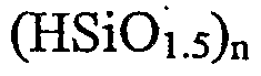
DISCLOSURE OF THE INVENTION The present invention includes a method of synthesizing and characterizing organic-inorganic HLED materials based on silsesquioxane architectures. These hybrid materials have the potential to combine the advantages of both molecular and polymer approaches to OLED applications. The silsesquioxane compounds incorporate at least one, and preferably multiple, functional moiety substituents within a single compound. The functional substituents are preferably selected from hole transport (HT), electron transport (ET), and emissive material (EM) moieties and combinations thereof. This offers considerable potential to optimize OLED properties, e.g. luminescence efficiency, brilliance, turn-on voltage, longevity, high density of HT, ET, and EM moieties, etc. The organic-inorganic HLED silsesquioxane material has the general formula (RSiOι.5)n wherein n typically ranges from 6 to 12 for discrete cage structures, but n can be much larger (up to about 100) in extended polymeric silsesquioxane structures, and R is selected from a plethora of functional groups including hole transport, electron transport, and emissive materials. The hybrids may be synthesized from a series of core polyhedral silsesquioxane intermediates having a variety of reactive substituent groups capable of reacting with functional groups having HT, ET, or EM properties. Examples of typical reactive substituent groups of silsesquioxane intermediates include, but are not limited to, hydrogen, vinyl, phenyl, substituted phenyl, stilbenyl, and substituted stilbenyl, where the phenyl substituents include, halo, amino, hydroxyl, vinyl, unsaturated alkyl, haloalkyl, silyl, etc. Some hybrids may also be synthesized using a direct sol-gel synthesis with R-Si(OCH2CH3)3 as a starting material.
One organic-inorganic HLED material having an octahedral silsesquioxane structure has the following general structure:
Figure imgf000008_0001
wherein Rj, R2, R3, R , R5, Re , R7, and Rs are selected from hole transport moieties, electron transport moieties, emissive material moieties, and curable groups including, but not limited to, epoxy, methacrylate, stryl, vinyl, propargyl and combinations thereof. The hybrid material preferably includes at least one HT, ET, or EM moiety. The curable groups are included to facilitate fabrication of multilayer devices, but would not necessarily be needed in a single layer device.
The present invention includes organic-inorganic HLED devices fabricated with an HLED material described above. Such devices typically include an anode containing a high work function metal, metal alloy, or metal oxide, a cathode containing a low work function metal or metal alloy, and a layer of the organic-inorganic luminescent material based upon the silsesquioxane structures described above, physically and thus electrically connected to the anode and cathode. The organic-inorganic HLED devices are preferably fabricated with a transparent substrate such as glass or clear plastic. The anode is preferably selected from gold, silver, copper, indium-tin oxide (ITO), fluorine-tin oxide (FTO), or other transparent conducting oxide or polymeric materials. Below about 50 nm, gold, silver, and copper layers are semi-transparent rendering them useful anode materials. The cathode is selected from calcium, magnesium, lithium, sodium, aluminum, and alloys thereof. The cathode may also be selected from mixtures of calcium, magnesium, lithium, sodium, and aluminum with halogen salts of group IA metals (Li, Na, K, Rb, Cs). For example, a commercially available Al/Li alloy (98.5% Al/1.5% Li) Al is relatively stable in air and has a work function similar to Ca. Similarly, LiF, CsF, and other salts can lower the work function when deposited at the Al organic interface.
The organic-inorganic HLED device can include multiple layers of organic- inorganic luminescent materials. Each layer can be based upon luminescent material having different functional moiety substituents selected from hole transport, electron transport, and emissive material moieties. For instance, the HLED device may include a layer having hole transport substituents, a layer having electron transport substituents with the hole and/or electron transport layer(s) also serving as the emissive component. Other substituents can be included to provide desired functional or physical characteristics, such as enhanced hydrophobicity, adhesive character, and dyes for color tuning to the HLED material. The HLED materials can also be designed to include multiple properties, such as balanced electron and hole transport as well as emissive properties.
The organic-inorganic HLED device can be fabricated with a single layer of the organic-inorganic luminescent material that contains hole transport, electron transport, and emissive material substituent moieties on a silsesquioxane structure. HLED devices can also be fabricated with multiple layers containing emissive, hole transport, and electron transport layers balanced to provide the desired luminescent properties.
BRIEF DESCRIPTION OF THE DRAWINGS Figure 1 is a schematic illustration of a typical OLED device configuration. Figure 2A is schematic illustration of a HLED device within the scope of the present invention containing a single layer of HLED material having integrated hole transport, electron transport, and emissive material properties.
Figure 2B is a schematic illustration of a HLED device within the scope of the present invention containing separate electron transport, emissive, and hole transport layers of HLED material.
Figure 3 is a graph of solution and thin film photoluminescence vs. wavelength for the hybrid material described in Example 2.
Figure 4 is a graph of current (A) and luminance (cd/m2) vs. voltage for a two- layer device fabricated with the inorganic-organic HLED material of Example 2.
DETAILED DESCRIPTION OF THE PREFERRED EMBODIMENTS The present invention is directed to new organic-inorganic HLED materials in which organic components are covalently linked to silsesquioxane inorganic (or organometallic) units. The organic-inorganic HLED silsesquioxane material has the general formula (RSiOι.5)n wherein n typically ranges from 6 to 12, but can range as high as 100, and R is selected from functional groups including hole transport (HT), electron transport (ET), and emissive (EM) materials. The hybrids may be synthesized from a core polyhedral silsesquioxane intermediate having reactive substituent groups capable of reacting with functional groups having HT, ET, or EM properties. Some hybrids may also be synthesized using a direct sol-gel synthesis with R-Si(OCH2CH3)3 as a starting material.
Presently preferred embodiments within the scope of the present invention rely on polyhedral octameric or cubic silsesquioxanes. The silsesquioxanes resemble skeletal frameworks found in crystalline forms of silica and particular zeolites. Bartsch, M.; Bornhauser, P.; Calzaferri, G. J. Phys. Chem. 1994, 98, 2817. Such structures can represent building blocks from which subsequent chemistry is used to prepare hybrids with the desired LED properties as described above. These structures are easily prepared in yields ranging from > 90% to 30%, from low cost starting materials. Their rigid framework offers many appealing properties that have been exploited by Feher et al. [Feher, F. ; Newman, D. A.; Walzer, J. F., J. Am. Chem. Soc, 1989, 111, 1741] to develop unique models of silica surfaces, by Calzaferri et al. [Bartsch et al., supra] as models of zeolites, by Klemperer et al. [Agaskar, P. A.; Day, V. W.; Klemperer, W. G, J. Am. Chem. Soc, 1987, 109, 5545] as unique sol-gel precursors, and by other groups for diverse applications. Access to these materials, especially the
Figure imgf000011_0001
series, is from extensive efforts by Agaskar [Agaskar, P. A., J. Am. Chem. Soc, 1989, 111, 6858; Agaskar, P. A., Inorg. Chem., 1992, 30, 2708; Agaskar, P. A., Colloids and Surfaces, 1992, 63, 131; and Agaskar, P. A., Synth. React. Inorg. Met.-Org. Chem., 1992, 20, 483]. Routes to the related [(R(CH3)2SiO)SiOι.5]8 and [(R(CH3)2SiO)SiOι.5]6/ιo cubes were reported by Hasegawa et al. [Hasegawa, I.; Motojima, S., J. Organomet. Chem., 1992, 373 and Hasegawa, I., J. of Sol-Gel Sci. and Tech., 1994, 2, 127] and German Patent No. DE 3837397, respectively.
Furthermore, functionalized cubic silsesquioxanes, where R = H, OSi(CH3)2H, CH=CH2, epoxy, and methacrylate, allow for incorporation into organic matrices providing hybrids with well defined, discrete nano-structures and tailorable properties [Sellinger, A.; Laine, R. M.; Chu, V.; Viney, C, J. Polymer Sci., Part A, Polymer Chemistry, 1994, 32, 3069; Sellinger, A.; Laine, R. M., Macromolecules, 1996, 26; Sellinger, A.; Laine, R. M., Chem. Mater., 1996, 8, 1592; and Laine, R. M.; Zhang, C, J. Organomet. Chem.,1996, 521, 199].
Combining electroluminescent functional groups with silsesquioxanes offers many unique and advantageous properties. This approach is based on coupling known and novel OLED functional groups with well-defined electronic properties (i.e. electron transport, hole transport, or emissive properties) with silsesquioxanes as shown below.
Figure imgf000011_0002
For example structure 1 wherein Rl5 R2, R3, R4, R5, Re, R , and Re are selected from hole transport, electron transport, emissive material, and curable moieties as described below. Examples of organic-inorganic HLED materials substituted with discrete hole transport, electron transport, and emissive moieties are illustrated below. Persons skilled in the art will appreciate that other HLED materials can be prepared having differentiating hole, electron transport, and emissive moieties.
Figure imgf000012_0001
Electron Transport HLED (2A)
Figure imgf000013_0001
Hole Transport HLED (2B)
Figure imgf000013_0002
Emissive HLED (2C)
There are several advantages of these HLED materials over molecular and polymer approaches currently described in the literature. For instance, these HLED materials may have molecular weights exceeding 3000 g/mol and thus are candidates for spray, dip and/or spin coating, or printing processes rather than vacuum sublimation, thereby providing a more cost effective application route. Other advantages, described in the following sections, include high temperature stability, ease of purification, high- density of HT, ET and EM moieties, and prevention of crystallization and aggregate formation to name a few.
As mentioned above, the HLED materials may be synthesized from polyhedral silsesquioxane intermediates having reactive substituent groups capable of reacting with functional groups having HT, ET, or EM properties. Several possible reactions that can be used for this purpose are illustrated generally below. Such reactions include, but are not limited to, high yield metal catalyzed hydrosilation, Heck, Suzuki, and Buchwald- Hartwig amination chemistry. In each reaction, it will be appreciated that one reactant will include the silsesquioxane intermediate and the other reactant will include the desired functional group.
Platinum catalyzed hydrosilation of silicon hydrides with double and triple bonds is shown below:
R3SiH + R\^ "R" ► R3Si-
Figure imgf000014_0001
Palladium catalyzed Heck reaction of vinyl groups with activated aromatic compounds is shown below, wherein X is Cl, Br, I, triflate, or other leaving group:
Figure imgf000014_0002
Palladium catalyzed Suzuki reaction of a halophenyl with activated aromatic compounds is shown below, wherein X is Cl, Br, I, triflate, or other leaving group: "Pd" Ar— X + Ar' — B(OR)2 > Ar— Ar'
Palladium catalyzed Buchwald-Hartwig amination reaction of activated aromatic compounds with aromatic amines is shown below:
R "Pd" /
Ar— X + Ar'— NRH > Ar— N
\ Ar'
Some hybrids may be synthesized using a direct sol-gel synthesis with R- Si(OCH2CH3)3 as a starting material, as shown below:
H+ or OH7H2θ
R-Si(OCH2CH3)3 > (RSiθ!.5)n sol-gel
where R is a hole transport moiety, electron transport moiety, emissive material moiety, or curable groups. Because some ET groiips may be sensitive to the acid or base reaction conditions used in sol-gel processing, the foregoing process may not be suitable for preparing ET functionalized silsesquioxane materials thus the former reaction methods are preferred.
This chemistry is straightforward, versatile, and may provide photo and/or thermally curable materials for multiple coating capabilities. The remaining double bond from the reaction of Si-H with triple bonds allows for each layer to be cured into an insoluble network immediately following deposition. For example, one can choose to: 1) synthesize a cube containing HT, ET, and EM moieties in a single cube (such as compound (3)) for a single step deposition process (Figure 2A) or 2) synthesize individual cubes containing only HT, ET, or EM moieties (such as compounds (2A)- (2C)) which can be deposited in successive layers (Figure 2B), or 3) any combination of these possibilities.
Figure imgf000016_0001
Figure 2A shows a HLED device 30 containing a single layer of HLED material 32 having integrated hole transport, electron transport, and emissive material properties. Using such a HLED material permits the device to be fabricated in a single step deposition process. Persons skilled in the art will appreciate that other HLED materials can be prepared having a combination emissive/hole transport moieties, emissive/electron transport moieties, or hole/electron transport moieties. Figure 2B is a schematic illustration of a HLED device 40 within the scope of the present invention containing separate hole transport 42, emissive 44, and electron transport 46 layers of HLED material.
The hybrids described in this invention may be purified by traditional polymer methods such as precipitation into a non-solvent. However, in contrast to polymers, hybrids based on silsesquioxanes may be purified by flash column chromatography, to provide materials with > 99.99% purity that is ideal for LED materials. As the cube materials can contain up to 40 wt. % silica, their thermal, hydrolytic and mechanical (e.g. abrasion resistance) properties are anticipated to be better than traditional OLED materials. The resulting materials are amorphous, transparent and thus have little tendency to crystallize over time. Furthermore, as the rigid rod HT, ET, and emissive moieties branch out from a three dimensional central core, little chance for alignment and aggregation exists thus minimizing the chance for eximer formation (charge traps) in devices. The high efficiency chemistry and resultant monodisperse spherical structures (sometimes referred to as dendrimers or starburst molecules) allows for precise control of functional groups (curing), processing parameters (viscosity), color tuning, electronic and optical properties, and materials morphology. HLEDs may be designed to be hydrophobic, as shown in compound (4), below, with fluoroalkyl groups, as adsorbed water is known to reduce OLED device lifetimes and efficiencies.
Figure imgf000017_0001
HLED compounds based on hydrido silsesquioxanes
The substituent R is preferably selected from hole transport, electron transport, and emissive material moieties. Although compound (4) is shown with four substituent R groups, it will be appreciated by persons having ordinary skill in the art that the type and number of substituent groups can be varied. In other words, the organic-inorganic HLED materials based upon the octahedral silsesquioxane structure can contain from 1 to 8 functional substituents, and the substituents can be the same or different.
The following are examples of typical electron transport moieties that can be used and/or chemically attached to the cubes (ET-HLED) within the scope of the present invention. The illustrated compounds are given by way of example only. Persons skilled in the art will appreciate that other known and novel electron transport moieties can be • used in the present invention, including but not limited to, organic compounds containing aromatic pyridines, quinolines, triazoles, oxadiazoles, dicyanoimidazoles, cyano aromatics, imino aromatics, and triazines or their combination.
Figure imgf000018_0001
pyridines quinolines triazoles oxadiazoles dicyanoimidazoles triazines Electron Transport Moieties
The following are examples of typical hole transport moieties that can be used and/or chemically attached to the cubes (HT-HLED) within the scope of the present invention. The illustrated compounds are given by way of example only. Persons skilled in the art will appreciate that other known and novel hole transport moieties can be used in the present invention, including, but are not limited to, organic compounds containing aromatic phosphines, aromatic amines, thiophenes (polythiophenes), silanes (polysilanes), and derivatives.
Figure imgf000018_0002
aromatic phosphenes aromatic amines thiophenes silanes
Hole Transport Moieties The following are examples of typical emissive material moiety substituents that can be used in the HLED materials within the scope of the present invention. The illustrated compounds are given by way of example only. Persons skilled in the art will appreciate that other known and novel emissive moieties can be used in the present invention.
Figure imgf000018_0003
poly(fluorenes) poly(m- or p-phenylene) poIy(phenylenevinylene) poly(phenyleneacetylenes'
Emissive Moieties Where R and R' = H, C, O, N, S, Si, Ge, fluoroalkanes, flourosilylalkanes, etc., and n is selected to optimize emissive properties and will typically range from 1 to 100, more preferably from 1 to 20.
The compounds shown above are examples of materials that can be used to make HLEDs. They are meant only to illustrate HLED materials within the scope of the invention and are not meant to limit the invention to the illustrated compounds.
EXAMPLES The following examples are given to illustrate various embodiments within the scope of the present invention. These are given by way of example only, and it is to be understood that the following examples are not comprehensive or exhaustive of the many embodiments within the scope of the present invention.
EXAMPLE 1 Product from the reaction of octavinylsilsesquioxane with 2-(4-bromophenyl)-5-
( 1 -naphthyl)- 1 ,3 ,4-oxadiazole.
Figure imgf000019_0001
Octavinylsilsesquioxane (1 g, 1.57 mmol), 2-(4-bromophenyl)-5-(l-naphthyl)- 1,3 ,4-oxadiazole (3.32 g, 9.46 mmol), palladium acetate (0.021 g, 0.095 mmol), and tris(o-tolyl)phosphine (0.072 g, 0.238 mmol) were added to a 25 mL schlenk flask equipped with stir bar, condenser, vacuum and argon gas source. The contents of the flask were evacuated and refilled with argon three times. Dry toluene (50 mL) and dry acetonitrile (10 mL) were added followed by triethylamine (1.45 mL, 10.4 mmol) and the solution was stirred for 48 hours at 100°C at which point thin layer chromatography indicated reaction completion. The solution was cooled to room temperature and poured into dichloromethane (200 mL). 5% HCl (100 mL) was added and the organic layer was extracted three times followed by brine (100 mL) three times. The organic layer was separated and dried with sodium sulfate and the volume was reduced to provide a tan solid (90% yield). The sample can be purified by column chromatography using a hexane/ethyl acetate system of 95/5. Alternatively, the solution was poured into 300 mL methanol and the precipitate was obtained via filtration. The powder was redissolved in THF or dichloromethane, filtered through a 0.45 um teflon membrane (Pall), and the powder again precipitated into methanol and collected by filtration followed by drying. Palladium dibenzylideneacetone [Pd2(dba)3], tri-t-butylphosphine (1/1 molar ratio) and N,N-dicyclohexylmethylamine may be used in place of palladium acetate, tris(o- tolyl)phosphine and triethylamine respectively. The former reagents allow for more mild reaction conditions, i.e., room temperature rather than 100°C and shorter reaction times (8 hrs). Size exclusion chromatography (SEC) revealed no starting material and a Mn = 2270 g/mol (2252 g/mol actual), and polydispersity index (PDI) of 1.10. Proton NMR was consistent with the title material and differential scanning calorimetry (DSC) revealed a glass transition (Tg) = 125°C.
EXAMPLE 2
Product from the reaction of octavinylsilsesquioxane with l-(w-tolyl- phenylamino)- 1 '-(p-bromophenyltolylamino)biphenyl.
Figure imgf000021_0001
This material was prepared using the procedure from Example 1 to give a yellow solid in 85% yield. Dilute solutions photoluminesce quite strongly in the presence of long wavelength light (around 360 nm) giving off a bright blue light. A solution photoluminescent spectral max of 488 nm was obtained using an excitation wavelength of 366 nm. The photoluminescence results for both solution and thin film are reported in Figure 3. Size exclusion chromatography (SEC) revealed no starting material and a M„ = 4920 g/mol (4750 g/mol actual), and polydispersity index (PDI) of 1.05. Proton NMR was consistent with the title material and differential scanning calorimetry (DSC) revealed a glass transition (Tg) = 152°C. Thermal gravimetric analysis (TGA) in air gave a ceramic yield of 11.2 % (theoretical ceramic yield = 10.1%).
The organic-inorganic HLED material prepared herein was fabricated into a two- layer device, such as that illustrated in Figure 1. Referring to Figure 1, the cathode layer 18 was an Al Li (98.5/1.5) alloy, layer 14 was an emissive (EM) material tris(8-hydroxy- quinolinato)aluminum (Alq3), layer 12 was the organic-inorganic HLED material prepared herein, anode layer 16 was indium tin oxide (ITO), and 22 was glass. Figure 4 is a graph of current (A) and luminance (cd/m2) vs. voltage for the fabricated device.
EXAMPLE 3 Product from the reaction of octavinylsilsesquioxane with 9,9-di-n-butyl-2- bromofluorene. + 5 equiv
Figure imgf000022_0002
Figure imgf000022_0001
The product was prepared using the procedure from Example 1 to give a yellow solid in 91% yield. Size exclusion chromatography (SEC) revealed no starting material and a Mn = 2825 g/mol (2015 g/mol actual), and polydispersity index (PDI) of 1.15. Proton NMR was consistent with the title material and differential scanning calorimetry (DSC) revealed a glass transition (Tg) = 102°C. Thermal gravimetric analysis (TGA) in air gave a ceramic yield of 26 % (theoretical ceramic yield = 23%).
EXAMPLE 5
Preparation of α-(bromo)-ω-(4-methoxyphenyl)-poly-2,7-(9,9-dioctylfluorene).
Figure imgf000022_0003
This monobrominated polymer was prepared according to a modified procedure to that described by Marsitzky et.al. (D. Marzitzky, M. Klapper, K. Mullen; Macromolecules, Vol. 32, No.25, 1999, 8685). 2-bromo-9,9-di-n-octylfluoreneboronic acid (1.0 g, 1.98 mmol), potassium fluoride (0.40 g, 6.93 mmol), palladium acetate (0.004g, 0.020 mmol), 2-dicyclohexylphosphanyl-biphenyl (0.014g, 0.040 mmol) were added to a 50 mL schlenk tube in a glove box. The tube was transferred to a schlenk line, and 7 mL of dry toluene and 7 mL DMAc were added. The solution was stirred at room temperature for 2-24 hrs at 80°C at which point excess 4-bromoanisole (1.2 mL) was added to endcap the polymer. The solution was further stiπed for 8 hrs at 80°C followed by precipitation in 200 mL methanol. The precipitate was dried, finely ground, and stkred with 5% HCl for 1 hour, filtered, rinsed with methanol and dried. The dried polymer was redissolved in minimal dichloromethane, and reprecipitated again in 200 mL methanol to afford 65% yield of dry polymer. A molecular weight of 4900 g/mol was determined by NMR endgroup analysis of the methoxy protons. GPC shows MW of 1200-6000 g/mol with PDI of 1.20-1.50 depending on the reaction time.
EXAMPLE 6
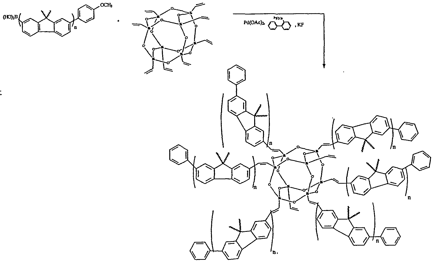
Preparation of a polyfluorene star polymer with a central silsesquioxane core.
Figure imgf000023_0001
α-(bromo)-ω-(4-methoxyphenyl)-poly-2,7-(9,9-dioctylfluorene) from Example 5 (lg, 0.20 mmol), octavinylsilsesquioxane (0.025g, 3.92 x 10"5 mol), palladium acetate (0.002 g, 0.01 mmol), and tris(o-tolyl)phosphine (0.007 g, 0.02 mmol) were added to a 25 mL schlenk flask equipped with stir bar, condenser, vacuum and argon gas source. The contents of the flask were evacuated and refilled with argon three times. Dry toluene (10 mL) and dry acetonitrile (or THF, dioxane) (2 mL) were added followed by triethylamine (0.035 mL, 0.25 mmol) and the solution was stirred for 48 hours at 100°C. The solution was cooled to room temperature and poured into cold methanol (20 mL) to precipitate a yellow solid. The solid is isolated by filtration, redissolved in dichloromethane (2 mL) and reprecipitated in methanol. GPC results are consistent with the anticipated structure. Alternatively palladium dibenzylideneacetone [Pd2(dba)3], tri-t-butylphosphine and N,N- dicyclohexylmethylamine may be used in place of palladium acetate, tris(o-tolyl)phos- phine and triethylamine respectively. The former reagents allow for more mild reaction conditions, i.e. 50°C rather than 100°C.
The present invention may be embodied in other specific forms without departing from its structures, methods, or other essential characteristics as broadly described herein and claimed hereinafter. The described embodiments are to be considered in all respects only as illustrative, and not restrictive. The scope of the invention is, therefore, indicated by the appended claims, rather than by the foregoing description. All changes that come within the meaning and range of equivalency of the claims are to be embraced within their scope.

Claims

CLAIMS:
1. An organic-inorganic HLED material comprising a silsesquioxane structure having at least one functional moiety substituent selected from hole transport, electron transport, and emissive material moieties.
2. An organic-inorganic HLED material according to claim 1, wherein the silsesquioxane structure comprises a plurality of functional moiety substituents selected from hole transport, electron transport, and emissive material moieties.
3. An organic-inorganic HLED material according to claim 1, wherein the silsesquioxane structure comprises a plurality of different functional moiety substituents selected from hole transport, electron transport, and emissive material moieties.
4. An organic-inorganic HLED material according to claim 3, wherein the functional moiety substituents include at least one emissive material moiety and at least one other functional moiety selected from hole transport and electron transport moieties.
5. An organic-inorganic HLED material according to claim 1, wherein the electron transport moiety is selected from aromatic pyridines, quinolines, triazoles, oxadiazoles, dicyanoimidazoles, triazines, cyano aromatics, imino aromatics, or their combination.
6. An organic-inorganic HLED material according to claim 1 , wherein the hole transport moiety is selected from aromatic phosphines, aromatic amines, thiophenes, silanes, or their combination.
7. An organic-inorganic HLED material according to claim 1, wherein the emissive moiety is selected from the following functional moiety substituent groups:
Figure imgf000026_0001
poly(fluorenes) poly(m- or p-phenylene) poly(phenylenevinylene) poly(phenyleneacetylenes'
Where R and R' = H, C, O, N, S, Si, Ge, fluoroalkanes, and flourosilylalkanes, and n is from 1 to 100.
8. An organic-inorganic HLED material comprising a polyhedral silsesquioxane structure having the following general structure:
Figure imgf000026_0002
wherein Ri, R2, R3, R4, R5, Re, R7, and Rg may be the same or different, and wherein at least one of Ri, R2, R3, RA, R5, Re, R7, and Rs is a hole transport moiety, electron transport moiety, or emissive material moiety.
9. An organic-inorganic HLED material according to claim 8, wherein at least one of Rj, R2, R3, R_t, R5, Re, R7, and Rs is selected from solubilizing and curable groups.
10. An organic-inorganic HLED material according to claim 9, wherein the solubilizing group is selected from fluoroalkanes and flourosilylalkanes.
11. An organic-inorganic HLED material according to claim 9, wherein the curable group is selected from epoxy, methacrylate, stryl, vinyl, propargyl and combinations thereof.
12. An organic-inorganic HLED material according to claim 8, wherein at least one of R], R2, R3, R , R5, R , R7, and Rs is selected from hydrogen, vinyl, phenyl, substituted phenyl, vinyl phenyl, and substituted vinyl phenyl, where the phenyl substituents include, halo, amino, hydroxyl vinyl, vinyl, unsaturated alkyl, and halo alkyl.
13. An organic-inorganic HLED material having the general formula
(RSiOι.5)n wherein n ranges from 6 to 100, R may be the same or different, and R is selected from hole transport moieties, electron transport moieties, emissive material moieties, curable moieties, and solubilizing moieties, wherein at least one R substituent is a hole transport, electron transport, or emissive material moiety.
14. An organic-inorganic HLED material according to claim 13, wherein n ranges from 6 to 12.
15. An organic-inorganic HLED material according to claim 13, wherein the curable moiety is selected from epoxy, methacrylate, stryl, vinyl, propargyl and combinations thereof.
16. An organic-inorganic HLED material according to claim 13, wherein the solubilizing moiety is selected from fluoroalkanes and flourosilylalkanes.
17. An organic-inorganic HLED device comprising: an anode containing a high work function metal or metal alloy; a cathode containing a low work function metal or metal alloy; a layer of organic-inorganic luminescent material comprising a silsesquioxane structure having at least one functional moiety substituent selected from hole transport, electron transport, and emissive material moieties, said luminescent material being electrically connected to the anode and cathode.
18. An organic-inorganic HLED device according to claim 17, further comprising a transparent substrate upon which the device is fabricated.
19. An organic-inorganic HLED device according to claim 17, wherein the anode is selected from gold, silver, copper, fluorine-tin oxide (FTO), and indium-tin oxide (ITO).
20. An organic-inorganic HLED device according to claim 17, wherein the anode is selected from poly(aniline) (PAN!) and poly(2,3-ethylenedioxy)thiophene (PEDOT).
21. An organic-inorganic HLED device according to claim 17, wherein the cathode is selected from calcium, magnesium, lithium, sodium, aluminum, and alloys thereof.
22. An organic-inorganic HLED device according to claim 17, wherein the cathode is selected from mixtures of calcium, magnesium, lithium, sodium, and aluminum with halogen salts of an alkaline earth metal.
23. An organic-inorganic HLED device according to claim 17, further comprising one or more additional layers of organic-inorganic luminescent material.
24. An organic-inorganic HLED device according to claim 17, wherein the organic-inorganic luminescent material comprises a plurality of different functional moiety substituents selected from hole transport, electron transport, and emissive material moieties.
25. An organic-inorganic HLED device according to claim 17, wherein the HLED device comprises a single layer of the organic-inorganic luminescent material and wherein the luminescent material contains hole transport, electron transport, and emissive material substituent moieties.
26. An organic-inorganic HLED device according to claim 17, wherein the HLED device comprises a layer of the organic-inorganic luminescent material having an emissive material substituent and a layer of the organic-inorganic luminescent material having an electron transport substituent.
27. An organic-inorganic HLED device according to claim 17, wherein the HLED device comprises a layer of the organic-inorganic luminescent material having an emissive material substituent and a layer of the organic-inorganic luminescent material having a hole transport substituent.
28. An organic-inorganic HLED device according to claim 17, wherein the electron transport moiety is selected from aromatic pyridines, quinolines, triazoles, oxadiazoles, dicyanoimidazoles, triazines, cyano aromatics, imino aromatics, or their combination.
29. An organic-inorganic HLED device according to claim 17, wherein the hole transport moiety is selected from aromatic phosphines, aromatic amines, thiophenes, silanes, or their combination.
30. An organic-inorganic HLED device according to claim 17, wherein the emissive moiety is selected from the following functional moiety substituent groups:
Figure imgf000030_0001
poly(fluorenes) poly(m- or p-phenylene) poly(phenylenevinylene) poly(phenyleneacetylenes"
Where R and R' = H, C, O, N, S, Si, Ge, fluoroalkanes, and flourosilylalkanes, and n is
Figure imgf000030_0002
PCT/US2001/041351 2000-07-14 2001-07-13 Organic-inorganic hybrid light emitting devices (hled) WO2002005971A1 (en)

Priority Applications (2)

Application Number Priority Date Filing Date Title
JP2002511899A JP3880518B2 (en) 2000-07-14 2001-07-13 Organic-inorganic hybrid light emitting device (HLED)
KR10-2003-7000480A KR20030043909A (en) 2000-07-14 2001-07-13 Organic-Inorganic Hybrid Light Emitting Devices (HLED)

Applications Claiming Priority (2)

Application Number Priority Date Filing Date Title
US09/616,561 2000-07-14
US09/616,561 US6517958B1 (en) 2000-07-14 2000-07-14 Organic-inorganic hybrid light emitting devices (HLED)

Publications (1)

Publication Number Publication Date
WO2002005971A1 true WO2002005971A1 (en) 2002-01-24

Family

ID=24470008

Family Applications (1)

Application Number Title Priority Date Filing Date
PCT/US2001/041351 WO2002005971A1 (en) 2000-07-14 2001-07-13 Organic-inorganic hybrid light emitting devices (hled)

Country Status (5)

Country Link
US (1) US6517958B1 (en)
JP (1) JP3880518B2 (en)
KR (1) KR20030043909A (en)
TW (1) TWI245793B (en)
WO (1) WO2002005971A1 (en)

Cited By (16)

* Cited by examiner, † Cited by third party
Publication number Priority date Publication date Assignee Title
JP2004006321A (en) * 2002-04-18 2004-01-08 Canon Inc Semiconductor hole injection material of organic light emitting device
WO2004060898A1 (en) * 2003-01-06 2004-07-22 Agency For Science, Technology And Research Quantum confined light-emitting dot material for low dimensional semiconductors
WO2005037955A1 (en) * 2003-10-15 2005-04-28 Nitto Denko Corporation Light emitting nanoparticle compositions
WO2006043678A1 (en) 2004-10-22 2006-04-27 Semiconductor Energy Laboratory Co., Ltd. Composite material and light emitting element
WO2007044138A1 (en) * 2005-10-07 2007-04-19 Dow Corning Corporation An electrophosphorescent organic light emitting diode formed using solvent soluble materials
US7285905B2 (en) 2001-08-31 2007-10-23 Sony Corporation Organic electroluminescence device comprising a silver alloy anode and method of manufacturing the same
WO2007136588A1 (en) * 2006-05-15 2007-11-29 Nitto Denko Corporation Light emitting devices and compositions
WO2009006550A1 (en) * 2007-07-05 2009-01-08 Nitto Denko Corporation Light emitting devices and compositions
WO2009064661A1 (en) * 2007-11-15 2009-05-22 Nitto Denko Corporation Light emitting devices and compositions
WO2010045263A2 (en) * 2008-10-13 2010-04-22 Nitto Denko Corporation Printable light-emitting compositions
WO2011002532A1 (en) * 2009-06-29 2011-01-06 General Electric Company Fluorene dimers and trimers and optoelectronic devices using the same
US7906724B2 (en) 2007-07-31 2011-03-15 Agency For Science, Technology And Research N-type conjugated materials based on 2-vinyl-4,5-dicyanoimidazoles and their use in organic photovoltaics
CN103052645A (en) * 2010-08-20 2013-04-17 亚当密茨凯维奇大学 Functionalized polyhedral octavinylsilsesquioxanes
CN108539036A (en) * 2017-03-06 2018-09-14 Tcl集团股份有限公司 A kind of electrode structure, QLED and preparation method that light extraction efficiency can be improved
US10134996B2 (en) 2004-10-29 2018-11-20 Semicondcutor Energy Laboratory Co., Ltd. Composite material, light-emitting element, light-emitting device, and manufacturing method thereof
DE102017111137A1 (en) 2017-05-22 2018-11-22 Novaled Gmbh Organic electroluminescent device

Families Citing this family (54)

* Cited by examiner, † Cited by third party
Publication number Priority date Publication date Assignee Title
US7820761B2 (en) 1999-08-04 2010-10-26 Hybrid Plastics, Inc. Metallized nanostructured chemicals as cure promoters
US20060263531A1 (en) * 2003-12-18 2006-11-23 Lichtenhan Joseph D Polyhedral oligomeric silsesquioxanes as glass forming coatings
US20060127583A1 (en) * 2003-12-18 2006-06-15 Lichtenhan Joseph D Polyhedral oligomeric silsesquioxanes and polyhedral oligomeric silicates barrier materials for packaging
US6861091B2 (en) * 2000-12-27 2005-03-01 Canon Kabushiki Kaisha Self-assembly of organic-inorganic nanocomposite thin films for use in hybrid organic light emitting devices (HLED)
CN100369285C (en) * 2001-02-06 2008-02-13 肖特股份公司 Method for producing light-emitting device and light-emitting device
US7008749B2 (en) * 2001-03-12 2006-03-07 The University Of North Carolina At Charlotte High resolution resists for next generation lithographies
JP2003086383A (en) * 2001-09-10 2003-03-20 Seiko Epson Corp Light-emitting device
JP3724725B2 (en) 2001-11-01 2005-12-07 ソニー株式会社 Manufacturing method of display device
US7776505B2 (en) * 2001-11-05 2010-08-17 The University Of North Carolina At Charlotte High resolution resists for next generation lithographies
CA2381833C (en) * 2002-04-16 2011-02-15 American Dye Source, Inc. Hybrid organic-inorganic light emitting polymers
US7531377B2 (en) * 2002-09-03 2009-05-12 Cambridge Display Technology Limited Optical device
US6936761B2 (en) * 2003-03-29 2005-08-30 Nanosolar, Inc. Transparent electrode, optoelectronic apparatus and devices
US7511217B1 (en) 2003-04-19 2009-03-31 Nanosolar, Inc. Inter facial architecture for nanostructured optoelectronic devices
US8119392B2 (en) * 2003-05-02 2012-02-21 The University Of North Carolina At Charlotte Biocompatible resists
US7605327B2 (en) * 2003-05-21 2009-10-20 Nanosolar, Inc. Photovoltaic devices fabricated from nanostructured template
US7462774B2 (en) * 2003-05-21 2008-12-09 Nanosolar, Inc. Photovoltaic devices fabricated from insulating nanostructured template
US7223517B2 (en) * 2003-08-05 2007-05-29 International Business Machines Corporation Lithographic antireflective hardmask compositions and uses thereof
KR100611157B1 (en) * 2003-11-29 2006-08-09 삼성에스디아이 주식회사 organic light-emitting device and fabrication method of the same
WO2005060671A2 (en) * 2003-12-18 2005-07-07 Hybrid Plastics Llp Polyhedral oligomeric silsesquioxanes and metallized polyhedral oligomeric silsesquioxanes as coatings, composites and additives
US20080249275A1 (en) * 2003-12-18 2008-10-09 Lichtenhan Joseph D Radiation shielding with polyhedral oligomeric silsesquioxanes and metallized additives
US20090085011A1 (en) * 2003-12-18 2009-04-02 Lichtenhan Joseph D Neutron shielding composition
KR100682859B1 (en) * 2004-01-27 2007-02-15 삼성에스디아이 주식회사 Polysilsesquioxane-based compound and organic electroluminescence device using the same
JP4963172B2 (en) * 2004-10-22 2012-06-27 株式会社半導体エネルギー研究所 Composite material and light emitting device
WO2006062177A1 (en) * 2004-12-06 2006-06-15 Semiconductor Energy Laboratory Co., Ltd. Composite material including organic compound and inorganic compound, light-emitting element and light-emitting device using the composite compound, and manufacturing method of the light-emitting element
JP4896411B2 (en) * 2005-02-18 2012-03-14 住友化学株式会社 Polymer compound and polymer light emitting device using the same
KR100657575B1 (en) 2005-03-23 2006-12-14 동양제철화학 주식회사 Novel polyfluorene-based polymer luminescent material and electroluminescent device comprising the same
KR101156426B1 (en) * 2005-08-25 2012-06-18 삼성모바일디스플레이주식회사 An silsesquioxane-based compound and an organic light emitting device comprising the same
KR101193179B1 (en) * 2005-08-26 2012-10-19 삼성디스플레이 주식회사 Organosiloxane compound and organic electroluminescence device comprsing the same
KR101193180B1 (en) * 2005-11-14 2012-10-19 삼성디스플레이 주식회사 A conducting polymer composition and an electronic device employing the layer obtained from the conducting polymer composition
KR101243917B1 (en) * 2005-12-19 2013-03-14 삼성디스플레이 주식회사 A conducting polymer composition and an electrical device employing the layer obtained from the conducting polymer composition
US20070225477A1 (en) * 2006-03-22 2007-09-27 General Electric Company Optoelectronic devices with multilayered structures
US7633220B2 (en) * 2006-03-22 2009-12-15 General Electric Company Optoelectronic devices with multilayered structures
US7830081B2 (en) * 2006-03-22 2010-11-09 General Electric Company Optoelectronic devices with multilayered structures
TW200811266A (en) * 2006-08-22 2008-03-01 Univ Nat Chiao Tung Electroluminescence polymer
JP2008106165A (en) * 2006-10-26 2008-05-08 Chisso Corp Inkjet ink and cured film formed using the ink
US9657040B2 (en) 2006-11-01 2017-05-23 Samsung Electronics Co., Ltd Cyclic siloxane compound, organic electroluminescence device, and use of the same
KR100813850B1 (en) * 2007-03-29 2008-03-17 삼성에스디아이 주식회사 Light emitting device
KR101420426B1 (en) * 2007-09-13 2014-07-16 엘지디스플레이 주식회사 Organic lighting emitting display device
EP2231814B1 (en) * 2008-01-11 2014-10-01 Dow Corning Corporation An electrochromic composition, a method of forming the electrochromic composition and an electrochromic apparatus
WO2009120434A1 (en) * 2008-03-26 2009-10-01 Dow Corning Corporation Silicone composition and organic light-emitting diode
WO2009152276A2 (en) 2008-06-10 2009-12-17 University Of North Carolina At Charlotte Photoacid generators and lithographic resists comprising the same
US8420235B2 (en) * 2009-06-04 2013-04-16 Nitto Denko Corporation Emissive diaryl acetylenes
WO2011016347A1 (en) * 2009-08-03 2011-02-10 株式会社アルバック Organic el device, electrode forming method for organic el device, organic el lighting device, and manufacturing method for organic el lighting device
WO2011149500A1 (en) 2010-01-07 2011-12-01 Nitto Denko Corporation Emissive compounds for organic light-emitting diodes
KR101489161B1 (en) * 2010-07-30 2015-02-06 주식회사 잉크테크 Method for manufacturing transparent conductive layer and transparent conductive layer manufactured by the method
WO2012111487A1 (en) * 2011-02-17 2012-08-23 住友化学株式会社 Compound having acceptor groups, and organic thin film and organic thin film element using same
JP6271853B2 (en) * 2013-04-03 2018-01-31 キヤノン株式会社 Organic light emitting device, display device, image information processing apparatus, and image forming apparatus
JP6374329B2 (en) * 2014-06-26 2018-08-15 出光興産株式会社 ORGANIC ELECTROLUMINESCENT ELEMENT, MATERIAL FOR ORGANIC ELECTROLUMINESCENT ELEMENT, AND ELECTRONIC DEVICE
CN106659950B (en) 2014-08-05 2020-04-21 信越化学工业株式会社 Oil composition for defoaming agent, method for producing same, and defoaming agent composition
CN105198917B (en) * 2015-08-26 2017-09-19 池州学院 A kind of organic inorganic hybridization fluorescent sensing material and its synthetic method and application
US11581487B2 (en) 2017-04-26 2023-02-14 Oti Lumionics Inc. Patterned conductive coating for surface of an opto-electronic device
EP3406752B1 (en) * 2017-05-22 2023-11-08 Novaled GmbH Method for preparing an electronic device
CN111495426A (en) * 2020-05-25 2020-08-07 西南科技大学 Polyaniline/perylene bisimide organic heterojunction photocatalyst, preparation method and application thereof
CN114672001B (en) * 2020-12-24 2024-01-09 中科院广州化学有限公司 Organic soluble high-conductivity multi-arm thiophene polymer and preparation method and application thereof

Citations (3)

* Cited by examiner, † Cited by third party
Publication number Priority date Publication date Assignee Title
US5635249A (en) * 1993-03-08 1997-06-03 Dow Corning Corporation Luminescent ceramic coatings
US6184304B1 (en) * 1998-02-06 2001-02-06 Dow Corning Corporation Photoluminescent material from hydrogen silsequioxane resin
US6284435B1 (en) * 1997-02-04 2001-09-04 Uniax Corporation Electrically active polymer compositions and their use in efficient, low operating voltage, polymer light-emitting diodes with air-stable cathodes

Family Cites Families (3)

* Cited by examiner, † Cited by third party
Publication number Priority date Publication date Assignee Title
US5527872A (en) * 1990-09-14 1996-06-18 At&T Global Information Solutions Company Electronic device with a spin-on glass dielectric layer
US5731117A (en) * 1995-11-06 1998-03-24 Eastman Kodak Company Overcoated charge transporting elements and glassy solid electrolytes
US6214937B1 (en) * 1999-03-26 2001-04-10 The University Of Akron Star-block polymers having multiple polyisobutylene-containing diblock copolymer arms radiating from a siloxane core and method for the synthesis thereof

Patent Citations (3)

* Cited by examiner, † Cited by third party
Publication number Priority date Publication date Assignee Title
US5635249A (en) * 1993-03-08 1997-06-03 Dow Corning Corporation Luminescent ceramic coatings
US6284435B1 (en) * 1997-02-04 2001-09-04 Uniax Corporation Electrically active polymer compositions and their use in efficient, low operating voltage, polymer light-emitting diodes with air-stable cathodes
US6184304B1 (en) * 1998-02-06 2001-02-06 Dow Corning Corporation Photoluminescent material from hydrogen silsequioxane resin

Cited By (30)

* Cited by examiner, † Cited by third party
Publication number Priority date Publication date Assignee Title
US10020460B2 (en) 2001-08-31 2018-07-10 Sony Corporation Electroluminescence device and display device
US8937428B2 (en) 2001-08-31 2015-01-20 Sony Corporation Organic electroluminescence device with silver alloy anode and method of manufacturing the same
US10522781B2 (en) 2001-08-31 2019-12-31 Sony Corporation Electroluminescence device and display device
US7285905B2 (en) 2001-08-31 2007-10-23 Sony Corporation Organic electroluminescence device comprising a silver alloy anode and method of manufacturing the same
US9722201B2 (en) 2001-08-31 2017-08-01 Sony Corporation Organic electroluminescence device and method of manufacturing the same
US9240564B2 (en) 2001-08-31 2016-01-19 Sony Corporation Organic electroluminescence device and method of manufacturing the same
JP2004006321A (en) * 2002-04-18 2004-01-08 Canon Inc Semiconductor hole injection material of organic light emitting device
WO2004060898A1 (en) * 2003-01-06 2004-07-22 Agency For Science, Technology And Research Quantum confined light-emitting dot material for low dimensional semiconductors
WO2005037955A1 (en) * 2003-10-15 2005-04-28 Nitto Denko Corporation Light emitting nanoparticle compositions
WO2006043678A1 (en) 2004-10-22 2006-04-27 Semiconductor Energy Laboratory Co., Ltd. Composite material and light emitting element
EP1802706A1 (en) * 2004-10-22 2007-07-04 Semiconductor Energy Laboratory Co., Ltd. Composite material and light emitting element
EP1802706A4 (en) * 2004-10-22 2012-09-26 Semiconductor Energy Lab Composite material and light emitting element
US10134996B2 (en) 2004-10-29 2018-11-20 Semicondcutor Energy Laboratory Co., Ltd. Composite material, light-emitting element, light-emitting device, and manufacturing method thereof
TWI406439B (en) * 2005-10-07 2013-08-21 Dow Corning An electrophosphorescent organic light emitting diode formed using solvent soluble materials
WO2007044138A1 (en) * 2005-10-07 2007-04-19 Dow Corning Corporation An electrophosphorescent organic light emitting diode formed using solvent soluble materials
US7993747B2 (en) 2006-05-15 2011-08-09 Nitto Denko Corporation Light emitting devices and compositions comprising lumophore-functionalized nanoparticles
WO2007136588A1 (en) * 2006-05-15 2007-11-29 Nitto Denko Corporation Light emitting devices and compositions
US8609258B2 (en) 2007-07-05 2013-12-17 Nitto Denko Corporation Light emitting devices and compositions
WO2009006550A1 (en) * 2007-07-05 2009-01-08 Nitto Denko Corporation Light emitting devices and compositions
US7906724B2 (en) 2007-07-31 2011-03-15 Agency For Science, Technology And Research N-type conjugated materials based on 2-vinyl-4,5-dicyanoimidazoles and their use in organic photovoltaics
WO2009064661A1 (en) * 2007-11-15 2009-05-22 Nitto Denko Corporation Light emitting devices and compositions
US20120273765A1 (en) * 2007-11-15 2012-11-01 Nitto Denko Corporation Light emitting devices and compositions
US8597803B2 (en) * 2007-11-15 2013-12-03 Nitto Denko Corporation Light emitting devices and compositions
US8721922B2 (en) 2008-10-13 2014-05-13 Nitto Denko Corporation Printable light-emitting compositions
WO2010045263A3 (en) * 2008-10-13 2010-07-08 Nitto Denko Corporation Printable light-emitting compositions
WO2010045263A2 (en) * 2008-10-13 2010-04-22 Nitto Denko Corporation Printable light-emitting compositions
WO2011002532A1 (en) * 2009-06-29 2011-01-06 General Electric Company Fluorene dimers and trimers and optoelectronic devices using the same
CN103052645A (en) * 2010-08-20 2013-04-17 亚当密茨凯维奇大学 Functionalized polyhedral octavinylsilsesquioxanes
CN108539036A (en) * 2017-03-06 2018-09-14 Tcl集团股份有限公司 A kind of electrode structure, QLED and preparation method that light extraction efficiency can be improved
DE102017111137A1 (en) 2017-05-22 2018-11-22 Novaled Gmbh Organic electroluminescent device

Also Published As

Publication number Publication date
KR20030043909A (en) 2003-06-02
TWI245793B (en) 2005-12-21
US6517958B1 (en) 2003-02-11
JP3880518B2 (en) 2007-02-14
JP2004506050A (en) 2004-02-26

Similar Documents

Publication Publication Date Title
US6517958B1 (en) Organic-inorganic hybrid light emitting devices (HLED)
CN101203538B (en) New luminescent compositions and their uses
JP4077796B2 (en) Biphenyl derivative and organic electroluminescence device employing the same
US6699599B2 (en) Deuterated semi-conducting organic compounds used for opto-electronic devices
US6815094B2 (en) Diphenyl anthracene derivatives and organic electroluminescent device employing the same
US6861091B2 (en) Self-assembly of organic-inorganic nanocomposite thin films for use in hybrid organic light emitting devices (HLED)
US7993747B2 (en) Light emitting devices and compositions comprising lumophore-functionalized nanoparticles
TWI280973B (en) Polymer compound and polymer light-emitting device using the same
US20180138413A1 (en) Dendrimer compound and organic luminescent device employing the same
JP4271772B2 (en) Luminescent compound and display element employing the same as coloring material
JP3823602B2 (en) Polymer fluorescent substance and organic electroluminescence device
JP2003213002A (en) Aromatic diamine-containing polymer compound and organic electroluminescent element using the same
CN101535319B (en) Cyclic siloxane compound, organic electroluminescent element, and use thereof
JP2001181618A (en) Method for producing polymer fluorescent substance and polymer light emitting element
US20070270592A1 (en) Phosphorescent multinuclear copper complex and organic electroluminescent device using the same
JP2008266425A (en) Sulfo group-containing cyclic polymer compound, method for producing the same and use thereof
US6841268B2 (en) Blue electroluminescent polymer and organic electroluminescence device using the same
CN1820061B (en) Mixtures of organic emissive semiconductors and matrix materials, their use and electronic components comprising said materials
JPWO2003050201A1 (en) Organic electroluminescence element material
WO2017153731A1 (en) Dibenzofuran and dibenzothiophene derivatives and organic light-emitting devices containing them
JPH09263754A (en) Organic electroluminescent element
JP2001226469A (en) New polymer, luminescent element material and luminescent element using the same
JP4924784B2 (en) Electron transport material and organic light emitting device using the electron transport material
JP2000215986A (en) Manufacture of organic electroluminescence element
JP2004002806A (en) Poly(silanylene-diethynyl arylene) and positive hole transport material

Legal Events

Date Code Title Description
AK Designated states

Kind code of ref document: A1

Designated state(s): JP KP KR US

AL Designated countries for regional patents

Kind code of ref document: A1

Designated state(s): AT BE CH CY DE DK ES FI FR GB GR IE IT LU MC NL PT SE TR

121 Ep: the epo has been informed by wipo that ep was designated in this application
WWE Wipo information: entry into national phase

Ref document number: 1020037000480

Country of ref document: KR

DFPE Request for preliminary examination filed prior to expiration of 19th month from priority date (pct application filed before 20040101)
WWP Wipo information: published in national office

Ref document number: 1020037000480

Country of ref document: KR

122 Ep: pct application non-entry in european phase
WWR Wipo information: refused in national office

Ref document number: 1020037000480

Country of ref document: KR