WO2004060898A1 - Quantum confined light-emitting dot material for low dimensional semiconductors - Google Patents

Quantum confined light-emitting dot material for low dimensional semiconductors Download PDF

Info

Publication number
WO2004060898A1
WO2004060898A1 PCT/SG2004/000004 SG2004000004W WO2004060898A1 WO 2004060898 A1 WO2004060898 A1 WO 2004060898A1 SG 2004000004 W SG2004000004 W SG 2004000004W WO 2004060898 A1 WO2004060898 A1 WO 2004060898A1
Authority
WO
WIPO (PCT)
Prior art keywords
compound according
organic functional
moieties
polymer
functional moiety
Prior art date
Application number
PCT/SG2004/000004
Other languages
French (fr)
Other versions
WO2004060898A8 (en
Inventor
Chaobin He
Yang Xiao
Junchao Huang
Khine Yi Mya
Original Assignee
Agency For Science, Technology And Research
Priority date (The priority date is an assumption and is not a legal conclusion. Google has not performed a legal analysis and makes no representation as to the accuracy of the date listed.)
Filing date
Publication date
Application filed by Agency For Science, Technology And Research filed Critical Agency For Science, Technology And Research
Publication of WO2004060898A1 publication Critical patent/WO2004060898A1/en
Publication of WO2004060898A8 publication Critical patent/WO2004060898A8/en

Links

Classifications

    • BPERFORMING OPERATIONS; TRANSPORTING
    • B82NANOTECHNOLOGY
    • B82YSPECIFIC USES OR APPLICATIONS OF NANOSTRUCTURES; MEASUREMENT OR ANALYSIS OF NANOSTRUCTURES; MANUFACTURE OR TREATMENT OF NANOSTRUCTURES
    • B82Y30/00Nanotechnology for materials or surface science, e.g. nanocomposites
    • BPERFORMING OPERATIONS; TRANSPORTING
    • B82NANOTECHNOLOGY
    • B82YSPECIFIC USES OR APPLICATIONS OF NANOSTRUCTURES; MEASUREMENT OR ANALYSIS OF NANOSTRUCTURES; MANUFACTURE OR TREATMENT OF NANOSTRUCTURES
    • B82Y10/00Nanotechnology for information processing, storage or transmission, e.g. quantum computing or single electron logic
    • CCHEMISTRY; METALLURGY
    • C07ORGANIC CHEMISTRY
    • C07FACYCLIC, CARBOCYCLIC OR HETEROCYCLIC COMPOUNDS CONTAINING ELEMENTS OTHER THAN CARBON, HYDROGEN, HALOGEN, OXYGEN, NITROGEN, SULFUR, SELENIUM OR TELLURIUM
    • C07F7/00Compounds containing elements of Groups 4 or 14 of the Periodic System
    • C07F7/02Silicon compounds
    • C07F7/21Cyclic compounds having at least one ring containing silicon, but no carbon in the ring

Definitions

  • This invention relates to low dimensional semiconductors and, in particular, to quantum confined light-emitting dot materials for low dimensional semiconductor systems.
  • excitons are elementary excitations in solids and arise due to Coulomb interaction between electrons and holes. Electron-hole pairs are typically formed when an excitation (such as a photon) is applied to a semiconductor. The electrons and holes are oppositely charged and (assuming a Coulomb interaction exists) a hydrogen-like bound pair (ie an exciton) is formed in place of a free electron-hole pair. In semiconductor materials, the excitons which are created extend cover many atomic sites in the crystal. These excitons can move quite freely through the crystal.
  • excitons In bulk semiconductors, excitons have generally low binding energies and, consequently, the electron-hole pairs dissociate relatively readily (even at room temperature). In low dimensional semiconductors, however, the confinement of the excitons leads to higher excitonic binding energies (so that excitons still exist at room temperature).
  • the free carriers or excitons are confined to a small region of space by potential barriers, and if the size of this region is less than the electron wavelength, the electronic states become quantized at discrete energy levels.
  • the materials can then exhibit quantum effects.
  • the two-dimensional electron gas in a quantum well (and other low dimensional systems) exhibits a large number of novel phenomena.
  • a large number of new electronic and opto-electronic devices have been made using quantum wells.
  • a thin layer of material of lower energy gap eg GaAs
  • a higher band-gap material eg Al x Ga 1-x As
  • the thickness of the middle GaAs layer is comparable to the de Broglie wavelength of electrons.
  • the electrons and holes enter into the quantum regime.
  • the particle wave function is reflected at the walls of the potential well existing at the two heterointerfaces and a standing wave pattern is thus formed.
  • the electrons are then allowed to stay in distinct sub-bands.
  • the resulting electron (hole) gas has two degrees of freedom and therefore constitutes a two-dimensional electron (hole) gas.
  • the fundamental absorption edge in a bulk semiconductor occurs when the photon energy equals the band gap energy. With a reduction of the thickness, the semiconductor enters into the quantum regime and the quantised energy levels move away from the nominal band edges. The absorption edge therefore shifts to higher energy and as the thickness is still further reduced, a further increase in the threshold is observed. This expected shift in the absorption edge has been observed in practice.
  • One feature of optical absorption and re-combination in all kinds of quantum well structures is that sharp excitonic features are present in the spectra even at room temperature.
  • the carrier density is quite large, as in a laser structure, the excitonic peak is completely bleached out; the absorption and re- combination are then due to transitions between valence sub-bands and conduction sub-bands.
  • these processes may also occur between the sub-bands belonging to the same band. For example, an electron in the ground sub-band in the conduction band may absorb a photon and go to the next higher sub-band belonging to the same conduction band. This is an inter-sub-band transition. Such processes may also take place between two sub-bands belonging to the valence band.
  • a one-dimensional system is known as a "quantum wire" in which the electron motion is confined along two dimensions and a one- dimensional electron gas is created.
  • quantum dot The theoretical ultimate limit of low dimensional structures is the quantum dot, in which the carriers are confined in all three directions. Therefore, a quantum dot can be thought of as a zero-dimensional electron gas. In quantum dots, the potential confines the particles in all three dimensions. The motion of the particles is then completely quantised and only discrete bound states are found. The energy levels correspond to the levels for an isolated atom. Therefore, a quantum dot is sometimes referred to as an artificial atom (or a super atom).
  • quantum dots have been formed as two-dimensional arrays in which the quantum dots are formed from modulation doped heterostructures such as GaAs/AIGaAs heterostructures.
  • the electrons are strongly confined to the heterointerface between GaAs and AIGaAs.
  • a periodic array of photoresist dots serves as the mask for further processing and, by employing a dry etching technique, deep grooves are cut all the way down to the active GaAs.
  • the etching leaves behind cylindrical mesas (eg about 500 nm in diameter).
  • Some of the electrons from the doped AIGaAs regions are trapped by the surface states at the open etched side walls and modify the potential profile electrostatically.
  • the boundaries of the confining potentials do not coincide with the physical side walls of the dot and the effective diameter of the quantum dots is then about 100 nm.
  • quantum dots have however presented a daunting challenge because the small dimensions required for quantum dots are at the limit of lithographic and semiconductor processing techniques and also because the dot interfaces should be kept defect-free in order to obtain the high-quality electronic properties that are required for device applications.
  • many efforts have been made to develop alternative routes for the fabrication of quantum dots that are based on the principle of self-organization.
  • single quantum dots would exhibit extremely sharp and atomic-like luminescence properties, the self-organization process results in inhomogeneous dot sizes. This causes considerable inhomogeneous line broadening to occur in larger dot ensembles and this has posed considerable limitations for devices applications.
  • Organic semiconductors with reduced dimensionality are also of growing interest owing to their expected unique features compared to the corresponding inorganic semiconductors.
  • Defect-free heterostructures can be more readily fabricated due to the weak Van der Waals interactions between organic molecules.
  • the smaller dielectric constant of organic molecules and polymers compared to inorganic semiconductors could result in strong Coulomb interactions between electrons and holes, leading to strong excitonic effects and large exciton binding energies.
  • Layered organic quantum-well heterostructures which are stacks of alternating thin films of different organic dye molecules, have been prepared (by ultra-high vacuum organic molecular beam deposition).
  • Such layered nanostructures eg formed of napthalene and perylene derivatives
  • Such layered nanostructures have been shown to exhibit the characteristics of multiple quantum wells with one- dimensional exciton confinement.
  • the resulting two-dimensional excitons in such crystalline multiple quantum wells have been shown to be spatially extended and to have relatively large binding energies.
  • the characteristic new discrete excitonic features in absorption or excitation spectra commonly observed in inorganic semiconductor multiple quantum wells were not observed in the layered organic nanostructures.
  • Certain linear conjugated copolymers have also been synthesized, characterized and used to investigate quantum confinement effects in semiconducting polymer heterostructures.
  • Theoretical studies have also been done on various aspects of the electronic and excitonic properties of quasi one-dimensional semiconducting polymer superlattices which are periodic copolymers. These theoretical studies have suggested that alternation of sufficiently long sequences of a lower energy gap polymer with those of a higher gap one could result in electron confinement in the segments of the chain with lower energy gap.
  • experimental attempts to produce such materials have not been successful as the materials have failed to show quantum size effects.
  • OLED's organic light emitting diodes
  • HLED's hybrid light emitting diodes
  • PCT/US01/41351 in the name of Canon Kabushiki Kaisha.
  • This specification discloses a range of organic-inorganic HLED materials based on silsesquioxane architectures.
  • the invention disclosed in this specification is directed to HLED light-emitting compositions in which electron transport (ET), hole transport (HT) and emissive material (EM) moieties are covalently linked to polyhedral silsesquioxanes.
  • the materials disclosed in the specification contain a silsesquioxane core to which multiple layers of organic-inorganic luminescent materials can be covalently linked (eg see pages 6 to 8).
  • Each layer can be based upon luminescent material having different function moiety substituents selected from hole transport, electron transfer and emissive material moieties.
  • the specification discloses a number of silsesquioxane-based compounds which incorporate certain organic moieties being electron transport (ET), hole transport (HT) and/or emissive material (EM) moieties.
  • organic moieties being electron transport (ET), hole transport (HT) and/or emissive material (EM) moieties.
  • ET electron transport
  • HT hole transport
  • EM emissive material
  • the specification states that these compounds can be used in the manufacture of single layer or multilayer light emitting devices. Where a single layer device is being formed, the relevant compounds each contain more than one type of organic moiety. For instance, each compound may contain ET and HT moieties, ET and EM moieties, HT and EM moieties, or ET, HT and EM moieties.
  • Devices containing a layer of such compounds can then exhibit a number of desired properties (eg electron transport and emission)
  • desired properties eg electron transport and emission
  • the specification states that different compounds are used for each layer, each compound having only one type of the above moieties.
  • one layer may be formed of compounds having only ET moieties.and another layer may be formed of EM moieties.
  • the choice of compounds is dependant upon the desired functionality of the device.
  • Devices containing multiple layers of such compounds may also exhibit a number of desired properties.
  • PCT/US01/41351 does not, however, make any mention of the disclosed materials having any quantum dot properties. Specifically, it does not make any mention of moieties having quantum dot properties (or quantum confinement effects). Nor does it make any mention of selecting the identity and location of the organic moieties in the compounds so that the compounds exhibit quantum dot properties. Similarly, the specification does not claim any benefits which could be achieved if such quantum confinement effects were produced.
  • Blending of two or more polymers is a well-established strategy for manipulating the physical properties and performance of materials without the need to synthesize new polymers.
  • blends of conjugated polymers are expected to be 'supramolecular' materials or 'alloys' in which novel properties not found in the homopolymers can emerge as a result of synergistic intermolecular interactions between components of the mixture, spatial confinement effects and self-organization.
  • Recent studies of blends of conjugated polymers have indeed shown them to exhibit novel supramolecular electronic, optoelectronic and photonic properties such as optical absorption modulation, photoinduced charge transfer, bipolar conductivity, enhanced photoconductivity, efficient energy transfer, enhanced electroluminescence and enhanced nonlinear optical properties.
  • the enhanced electroluminescence (EL) from blends of conjugated polymers has been described in some recent reports. The mechanism of the observed EL enhancement has been attributed to Forster-type energy transfer from high band-gap polymer to low band-gap polymer.
  • the observed EL enhancement in polymer blends is caused primarily from the spatial confinement of excitons which leads to improved exciton stability and electron-hole recombination efficiency. Larger EL enhancement in blended materials can be expected if both larger exciton confinement and excitation energy transfer could be facilitated. It is however the aggregation of the light emitting medium which limits further improvement of quantum efficiency.
  • the present invention is directed towards providing novel organic quantum dot semiconductor materials having desired particle sizes, quantum confinement in three dimensions, high PL quantum efficiencies, stable electroluminescent emissions, non-aggregation (or reduced aggregation) in solid state for photo- and electron-excited emissions, narrow emission widths, facile synthesis methods and processes, and tailorable properties based on structure modification.
  • Such materials would combine many of the advantages of inorganic semiconductor materials with organic and polymeric semiconductor materials. For instance, like organic and polymeric materials, these materials would generally have molecular weights which are typically more than 2500g/mol. Thus, they could be fabricated into devices via spin coating or printing processes rather than vacuum sublimation, thereby providing a more cost-effective application route. On the other hand, like inorganic materials, such materials would be thermally stable, easy to purify, have narrow molecular weight polydispersity, and have precise particle sizes with unique properties. Furthermore, these organic quantum dot materials would have intrinsic structures which not only inhibit crystallization (better than many inorganic semiconductor materials) but they would also inhibit aggregation (better than many other organic and polymeric semiconductor materials).
  • the invention is also directed to designing, synthesizing and characterizing organic or hybrid compounds with a core structure and multiple surrounding layers.
  • Either the core or multiple layers typically have precise sizes and different functions.
  • the multiple layers generally give rise to one or more effects such as quantum confinement, improved solubility, suitable energy band gap for energy transfer, photoluminescent or electron luminescent, spacer function of separation of different layers or functions, etc.
  • a quantum dot semiconductor compound comprising an inner core adapted to have 3 or more substituents attached thereto, wherein at least one of the substituents includes an organic functional moiety adapted to exhibit three dimensional quantum confinement.
  • the inner core is preferably formed of a carbon atom, a silicon atom, or a polyhedral silsesquioxane structure.
  • An inner core formed of a polyhedral silsesquioxane structure is particularly preferred.
  • Such a polyhedral silsesquioxane structure may have a general formula of (SiO- ⁇ . 5 ) n , wherein n ranges from 6 to 100, preferably from 6 to 12.
  • the silsesquioxane structure is typically an octahedral or cubic structure.
  • the inner core may have up to 8 substituents, each of which may include one of said organic functional moieties. It is also possible that the substituents may each have more than one of the organic functional moieties. In a preferred embodiment, each of the substituents surrounding the inner core consists only of one of said organic functional moieties. In this embodiment, the energy band gap of the organic functional moiety is less than the energy band gap of the inner core.
  • the functional moieties surrounding the inner core may all be the same. However, they need not all the same. There may be some which are the same and others which are different, or alternatively, they may all be different. It is however generally preferred that the said functional moieties within a given compound are the same.
  • each organic functional moiety may have an additional functional group attached thereto, and each such functional group has an energy band gap greater than the band gap of the organic functional moiety to which it is attached.
  • Each of these additional functional groups may in turn have a further functional group attached to it. This ensures exciton confinement to the region of said functional moiety.
  • each of the substituents includes a functional moiety and an additional functional group attached thereto.
  • a compound can be viewed as having 2 layer shells about the inner core - an inner layer shell formed of the functional moieties of the substituents, and an outer layer shell being formed of the additional functional groups of the substituents. Accordingly, the inner layer shell will have a lower band gap than the outer layer shell and quantum confinement will occur in the region of the inner layer shell.
  • each said substituent consists of 2 or more of said organic functional moieties. These 2 or more moieties may be attached together in blocks.
  • These blocks may be separated by one or more additional functional groups (or blocks of such functional groups), wherein the functional groups have a higher energy band gap than that of the organic functional moieties. It is also possible that a number of single organic functional moieties exist within the substituent and which are separated by one or more of the abovementioned functional groups.
  • a terminal end of each substituent comprises an alkyl chain.
  • the additional functional groups, the further functional groups and/or the alkyl chains can be selected from a large range of groups. Their selection will depend upon the desired purposes or uses of the compounds and, consequently, they may be chosen for their desired properties, such as quantum confinement, hydrophilicity (to improve water solubility), improved solubility in organic solvents, energy band gap (for desired energy transfer), photoluminescence, electrical luminescence, spacer function (for separating different layers) etc.
  • Each substituent may comprise a number of said functional groups which again can be chosen for their desired properties. Accordingly, each substituent may in fact consist of a polymer chain wherein the polymer chain comprises the functional moiety and the attached one or more functional groups.
  • the compound may be structured so that (instead of the functional moieties being attached directly to the inner core) the substituents may include a functional group attached to the inner core and the functional moiety attached to the functional group.
  • the functional group will have a higher energy band gap than the functional moiety attached thereto.
  • each substituent comprises a polymer and the organic functional moiety forms part of the polymer.
  • the organic functional moiety may be connected to the inner core in which case the energy band gap of the organic functional moiety is lower than that of both the inner core and a monomeric unit adjoining the organic functional moiety.
  • the organic functional moiety may be positioned between 2 monomeric units of the polymer, both of which have energy band gaps higher than that of the organic functional moiety.
  • Each polymer may comprise 2 or more of said organic functional moieties.
  • moieties may be attached together in blocks or they may be located as single units along the polymer chain. In either case, they will preferably be bound on either side by monomeric units of the polymer which have energy band gaps higher than that of the organic functional moiety.
  • the above polymers are preferably oligo-conjugated polymers, such as oligo-polyphenylene and oligo-polythiophene.
  • all of the substituents include one of said organic functional moieties attached to the inner core, said inner functional moieties forming a first layer shell about said inner core. It is further preferred that all of the substituents also include an additional functional group attached to the organic functional moiety, thereby forming a second layer shell about the inner core.
  • Each additional functional group may be a polymer, preferably an oligo- conjugated polymer, such as oligo-polyphenylene and oligo-polythiophene.
  • Each substituent may further include a further functional group attached to the additional functional group, thereby forming a third layer shell about said inner core. Such a further functional group may be an alkyl chain.
  • the inner core is preferably a polyhedral silesquioxane structure having from 6 to 12 substituents attached thereto. It is particularly preferred that the polyheydral silesquioxane structure has substituents selected from the group consisting of: an organic functional moiety adapted to exhibit three-dimensional quantum confinement; such an organic functional moiety having a functional group attached thereto, said organic functional moiety having a lower energy band gap than the functional group; a functional group having such a functional moiety attached thereto, said functional group having a higher energy band gap than the organic functional moiety; and - a polymer which includes such an organic functional moiety wherein any monomeric unit which adjoins the organic functional moiety has a higher energy band gap than the organic functional moiety. It is particularly preferred that the substituents are such polymers.
  • oligo-conjugated polymers are particularly preferred in this regard.
  • the polymers may include an alkyl chain attached thereto, typically at a terminal end of the polymer.
  • the polymer may comprise 2 or more of the organic functional moieties. These 2 or more functional moieties are preferably attached together in blocks, typically of 2-9 units.
  • the polymer may comprise only 1 organic functional moiety. In either case, the functional moiety, or block of moieties, is typically positioned between monomeric units having energy band gaps higher than that of the organic functional moiety.
  • the functional moiety may be positioned in any desired location within the substituent. For instance, it may be attached to the inner core. Alternatively, it could be located between 2 monomeric groups in the polymer chain, or it could be at a distant end of the chain. In such embodiments, any functional group or monomeric group adjoining the organic functional moiety will typically have an energy band gap which is greater than that of the functional moiety. This is so as to ensure exciton confinement in the region of the functional moiety.
  • the polymer may comprise, in addition to said organic functional moiety, 2 or more monomeric units which may be the same or different.
  • the compound may have the structural formula:
  • R1 , R2...Rn can consist of aromatic ring structures and multi aromatic ring structures arranged so that a structure of low energy band gap is located either between the inner core and a structure of higher energy band gap, or between two such structures of higher energy band gap.
  • aromatic ring structures may be selected from the group consisting of phenyl, substituted phenyl, vinyl phenyl, substituted vinyl phenyl, arylene, heteroarylene, fused ring arylene, fused ring heteroarylene, alkoxy, alkylene, vinylene, ethynyl, and combinations thereof.
  • the aromatic ring structures may be substituted by one or more functional groups, including electron-donating groups, electron-withdrawing groups, solubilising groups, silicon containing groups, metal containing groups, or Group III to V element containing groups or epoxy.
  • the aromatic ring structures specifically include substituted phenyl wherein the phenyl substituents are selected from the group consisting of hydrogen, fluorine, chlorine, bromine, amino, alkoxy and alkylene.
  • a preferred embodiment of the above aspect of the invention relates to a hybrid light-emitting device material having a core structure and multiple surrounding layers, wherein the core structure is based on silsesquioxane architectures.
  • the multiple layers may be formed of the same or different organic materials which are selected for their ability to provide one or more of the following effects, quantum confinement, improved solubility, suitable energy band gap for energy transfer, photoluminescence or electron luminescence, and spacer function of separation of different layers or functions.
  • the above multi-layered quantum dot compound can be synthesized from a series of core polyhedral silsesquioxane intermediates having a variety of reactive substituent groups to provide the starting point of subsequent growth of multiple layers.
  • Examples of typical reactive substituent groups of silsesquioxane intermediates include, but are not limited to, hydrogen, vinyl, phenyl, substituted phenyl, where the phenyl substituents include halo, amino, hydroxyl, vinyl, unsaturated alkyl, haloalkyl, silyl, etc.
  • the core-multiple-layer structure can be realized either via layer by layer additions to the core structure or a one step reaction combining core and pre-prepared multiple layer components.
  • One such organic quantum dot material having an octahedral silsesquioxane structure has the structure set out above, namely: Rn
  • R1 , R2, R3,KRn are the multiple layer components which can be any group, such as, but not limited to, aromatic ring or multi-aromatic ring
  • the aromatic ring may be selected from the group consisting of arylene, heteroarylene, fused-ring arylene and fused-ring heteroarylene, alkoxy, alkylene, vinylene, ethynyl, and combinations of above moieties.
  • the above moieties can be substituted by one or more functional groups such as electron-donating or electron-withdrawing groups, solubilising groups, silicon containing, metal containing, or lll-V element containing moieties, and epoxy.
  • the above components can be synthesized from a series of core polyhedral selsequioxane intermediates having a variety of reactive substituent groups to provide the starting points of subsequent growth of multiple layers.
  • typical reactive substituent groups of silsequioxane intermediates include, but are not limited to, hydrogen, vinyl and substituted phenyl.
  • the phenyl subsituents may include halo, amino, hydroxyl, vinyl, unsaturated alkyl, haloalkyl, silyl etc.
  • the components can be synthesized by multiple reactions, adding the layers to the core one at a time, or by a one-step reaction which combines the core with pre-prepared multi functional group components, such as polymers.
  • the inner core is formed of a cubic polyhedral digomeric silsesquioxand (POSS) structure.
  • the substituents are added to the inner core by grafting the eight corners of the POSS structure with oligo poly-phenylene or oligo poly-thiophene (e.g. POSS-2Ph, POSS-3Ph, POSS-4PH and POSS-Ph-2Th).
  • oligo poly-phenylene or oligo poly-thiophene e.g. POSS-2Ph, POSS-3Ph, POSS-4PH and POSS-Ph-2Th.
  • the size of the quantum dot increases with increase in the number of phenyls or thiophenes grafted onto the structure.
  • the quantum dot size is smaller than the Bohr radius of the bulk exciton (which is generally about 2nm for organic semiconductor materials), the electronic excitation is strongly confined in all 3 dimensions.
  • the colour of the quantum dot emission can be controlled both by manipulating the quantum dot size and by using different band gap materials. For example, if the oligo polyphenylene is substituted with oligo polythiophene (which has a lower band gap energy), the UV absorption and the photoluminescence spectra undergo a red shift to longer wavelength. Similarly, for POSS-3Ph, the photoluminescence peak is at about 380nm, whereas for POSS-Ph-2Thio, the photoluminescence peak is at about 500nm.
  • the compounds of a preferred embodiment of this invention can be considered as being 3-layered structures comprising an inner core (such as a polyhedral silsequioxane structure), a middle layer of oligo-conjugated polymers and an outer layer of alkyl chains.
  • the energy band gap of the relevant oligo- conjugated polymers is less than that of both the inner core and the relevant alkyl chains.
  • the electrons are thereby confined between the inner core and the outer alkyl chains.
  • the compounds of this invention are able to be formed having particular particle sizes, quantum confinement in 3 dimensions, thermal stability, high photoluminescent quantum efficiencies, stable electroluminescent omissions, non-aggregation of particles and narrow emission widths. The methods of synthesizing these compounds are relatively straightforward.
  • the compounds can be tailored to have certain desired properties by modifying or varying the structure of the compounds. Accordingly, the compounds facilitate colour-tuneability and property tailorability of the devices made from them. Therefore, the compounds of the present invention have great potential in the field of semiconductor technology and other fields, including electroluminescent devices and diode lasers, wherein these materials can be used as emission materials or charge carrier transporting materials. Furthermore the compounds of this invention can be used as host or guest materials for energy transfer or quantum confinement for other materials. They also have applications in photovoltaic cells and as biosensors and biodetectors (e.g. fluorescent biological labels).
  • Figure 1 is a graph showing photoluminescence of a compound 4 thin film and dilute solution in the THF.
  • Figure 2 is a graph showing photoluminescence of compound 5 thin film and dilute solution in the THF.
  • Figure 3 is a graph showing photoluminescence of blending a conventional polymer (having a higher band gap than compound 5) with compound 5 in thin film.
  • Figure 4 is a graph showing current against voltage in respect of a double layer electroluminescent device ITO/HTL/3a/Ca.
  • Figure 5 is a graph showing time resolved photoluminescence for a film of compound 5, a film in matrix (1 :3wt) and a dilute solution in THF.
  • the core structure is based on polyhedral octameric or cubic silsesquioxanes. Such a structure can represent building blocks from which subsequent reaction can add multiple layers one by one with desired properties or functions on each layer.
  • the core structures are easily prepared in high yields from low cost starting materials which are commercially available. This rigid framework offers many appealing properties. Not only does it provide the crucial core structure with eight or more starting points to enable growth into a sphere-like quantum dot material, but it also enables development of unique models of silica surfaces which have special advantages in semiconductors.
  • Ri is preferably hydrogen, phenyl, substituted phenyl or vinyl, wherein the phenyl substituents include halo, amino, hydroxyl, vinyl, unstaturated alkyl, haloalkyl, silyl, etc.
  • the organic quantum dot materials can be synthesized from polyhedral silsesquioxane intermediates having reactive substituent groups capable of reacting with other functional groups to form either the core-multiple-layers or core-first-layer structures followed by subsequent reactions adding layers one by one.
  • Several possible reactions that can be used for this purpose are illustrated generally below. Such reactions include, but are not limited to, metal catalyzed hydrosilation, Gragnard reaction, Heck reaction, Suzuki coupling reaction, and Buchwald Hartwig amination.
  • the multiple layers have a variety of functions or results, including but not limited to, quantum confinement, improved solubility, matching of energy band gap for energy transfer, photoluminescence or electroluminescence, electron or hole transporting or injection, isolation of different layers or functions, etc.
  • the components of each layer can be selected from conventional structures with desired properties.
  • the emissive layer can be formed of any arylene, heteroarylene, fused-ring arylene and fused-ring heteroarylene.
  • the solubilising or quantum confinement layer and spacer can be formed of any of alkoxy, alkylene, or single atom such as S, O, N, Si, metal, etc.
  • the graph of Figure 1 contains 2 curves showing the photoluminescence of compound 4 both in solution and as a film.
  • the graph of Figure 2 also contains 2 curves which represent the photoluminescence of compound 5, both in solution and as a film.
  • the well matched PL spectra of the solution and the film in each case indicates that there is no significant aggregation of the compound in the solid state.
  • FIG. 3 shows a blending system in which there is an effective energy transfer from the higher band gap material (ie a polymer) to the material of compound 5 which has lower band gap than the polymer.
  • the PL peak of compound 5 (486nm) remains unchanged as polymer content increases and PL quantum gets higher. This demonstrates the intrinsic three dimensional quantum confinement exhibited by compound 5. Materials without intrinsic quantum confinement will have their PL peak blue shift as blending with higher band gap materials occurs. This is because the higher band gap surrounding material will help lower band gap molecules separate from each other causing their excitons to become more and more localized.
  • Figure 4 is a graph showing the change in current/luminescence as the voltage increases across a double layer device formed of ITO/HTL/3a/Ca (where 3a is the compound 3a referred to above).
  • This graph shows the preliminary results of the double layer electroluminescent device.
  • the substantial delay in the increase of luminescence compared to the current suggests that the electron injection and transporting are the crucial step. Consequently, better performance is expected if an ETL (electron transporting layer) is added between the cathode and compound 3a. This indicates that the materials can be used as emissive candidates.
  • ETL electron transporting layer
  • Figure 5 is a graph showing time resolved photoluminescence of a film of the compound 5, a film in matrix of compound 4 (1 :3 wt), and a dilute solution in THF.
  • the photoluminescent decay of the solution, the film in matrix (higher band gap material), and the film all have similar decay times (150ps-180ps). This suggests that the carriers are localized even in the film sample, again demonstrating the intrinsic quantum confinement in compound 5.
  • Conventional polymers normally show a big difference in photoluminescence depending on whether they are in the form of a film (e.g. about 100ps) or a solution (e.g. about 1000ps).
  • Compound 1 can be formulated as shown below:
  • Compound 3 can be formulated as shown below:
  • Compound 2 can be formulated as shown below:
  • Compound 4 can be formulated as shown below:
  • Butyllithium (1.2M in hexane) (2.6ml) was added dropwise into a solution of compound C (1.0962g, 2.357mmol 0.4M in dry THF) at -78°C under Argon and stirring. After 1 hr, a solution, prepared by BrCH2CH2Br (0.8648g, 4.6mmol) and
  • Compound 5 can be formulated as shown below:
  • Table 1 shows the results of analyses performed on the compounds produced in the Examples. For instance, Table 1 shows the particle sizes of the compounds, determined from wide-angle XRD, compared with the size of the compounds determined by theoretical calculations. The Table also shows the compounds' molecular weights (g/mol) from GPC and absolute photoluminescent quantum efficiencies (PLQE) from the integrating sphere.
  • Table 2 shows the time resolved photoluminescence for dilute solutions of compounds 2, 3 and 4 in THF.

Abstract

A quantum dot semiconductor compound comprising an inner core adapted to have 3 or more substituents attached thereto, wherein at least one of the substituents includes an organic functional moiety adapted to exhibit three dimensional quantum confinement.

Description

QUANTUM CONFINED LIGHT-EMITTING DOT MATERIAL FOR LOW DIMENSIONAL SEMICONDUCTORS
Field of the Invention
This invention relates to low dimensional semiconductors and, in particular, to quantum confined light-emitting dot materials for low dimensional semiconductor systems.
Background to the Invention
Low dimensional inorganic semiconductor systems have been of much scientific and technological interest in the past three decades due to their potential applications in products such as diode lasers, optical modulators, self- electrooptical devices, optical waveguide switches and cavity-less nonlinear optical bistability.
Compared to bulk semiconductors, low dimensional semiconductors (ie nanostructures) exhibit novel and/or modified electronic and optical properties that can be attributed to spatial confinement of charge carriers or excitons. Excitons are elementary excitations in solids and arise due to Coulomb interaction between electrons and holes. Electron-hole pairs are typically formed when an excitation (such as a photon) is applied to a semiconductor. The electrons and holes are oppositely charged and (assuming a Coulomb interaction exists) a hydrogen-like bound pair (ie an exciton) is formed in place of a free electron-hole pair. In semiconductor materials, the excitons which are created extend cover many atomic sites in the crystal. These excitons can move quite freely through the crystal. In bulk semiconductors, excitons have generally low binding energies and, consequently, the electron-hole pairs dissociate relatively readily (even at room temperature). In low dimensional semiconductors, however, the confinement of the excitons leads to higher excitonic binding energies (so that excitons still exist at room temperature).
In the abovementioned low dimensional semiconductors, the free carriers or excitons are confined to a small region of space by potential barriers, and if the size of this region is less than the electron wavelength, the electronic states become quantized at discrete energy levels. The materials can then exhibit quantum effects. The two-dimensional electron gas in a quantum well (and other low dimensional systems) exhibits a large number of novel phenomena. As a consequence, a large number of new electronic and opto-electronic devices have been made using quantum wells. In a quantum well, a thin layer of material of lower energy gap (eg GaAs) is sandwiched between 2 thick layers of a higher band-gap material (eg AlxGa1-xAs). The thickness of the middle GaAs layer is comparable to the de Broglie wavelength of electrons. In quantum wells, the electrons and holes enter into the quantum regime. The particle wave function is reflected at the walls of the potential well existing at the two heterointerfaces and a standing wave pattern is thus formed. The electrons are then allowed to stay in distinct sub-bands. The resulting electron (hole) gas has two degrees of freedom and therefore constitutes a two-dimensional electron (hole) gas.
The fundamental absorption edge in a bulk semiconductor occurs when the photon energy equals the band gap energy. With a reduction of the thickness, the semiconductor enters into the quantum regime and the quantised energy levels move away from the nominal band edges. The absorption edge therefore shifts to higher energy and as the thickness is still further reduced, a further increase in the threshold is observed. This expected shift in the absorption edge has been observed in practice.
One feature of optical absorption and re-combination in all kinds of quantum well structures is that sharp excitonic features are present in the spectra even at room temperature. When the carrier density is quite large, as in a laser structure, the excitonic peak is completely bleached out; the absorption and re- combination are then due to transitions between valence sub-bands and conduction sub-bands. In addition to the usual band-to-band transitions, these processes may also occur between the sub-bands belonging to the same band. For example, an electron in the ground sub-band in the conduction band may absorb a photon and go to the next higher sub-band belonging to the same conduction band. This is an inter-sub-band transition. Such processes may also take place between two sub-bands belonging to the valence band.
Also, in a quantum well or other low-dimensional system, the confinement of the carriers (eg free electrons and holes) leads to relatively high excitonic binding energies so that excitons persist even at room temperature. In bulk semiconductors, on the other hand, higher temperatures often result in disassociation of excitons (owing to the relatively low binding energy of the exciton).
The tremendous success of two-dimensional quantum wells has prompted further enquiry into systems having still lower dimensionality (eg one dimension and zero dimension). A one-dimensional system is known as a "quantum wire" in which the electron motion is confined along two dimensions and a one- dimensional electron gas is created.
The theoretical ultimate limit of low dimensional structures is the quantum dot, in which the carriers are confined in all three directions. Therefore, a quantum dot can be thought of as a zero-dimensional electron gas. In quantum dots, the potential confines the particles in all three dimensions. The motion of the particles is then completely quantised and only discrete bound states are found. The energy levels correspond to the levels for an isolated atom. Therefore, a quantum dot is sometimes referred to as an artificial atom (or a super atom).
Generally, quantum dots have been formed as two-dimensional arrays in which the quantum dots are formed from modulation doped heterostructures such as GaAs/AIGaAs heterostructures. The electrons are strongly confined to the heterointerface between GaAs and AIGaAs. A periodic array of photoresist dots serves as the mask for further processing and, by employing a dry etching technique, deep grooves are cut all the way down to the active GaAs. The etching leaves behind cylindrical mesas (eg about 500 nm in diameter). Some of the electrons from the doped AIGaAs regions are trapped by the surface states at the open etched side walls and modify the potential profile electrostatically. Thus, the boundaries of the confining potentials do not coincide with the physical side walls of the dot and the effective diameter of the quantum dots is then about 100 nm.
Other known quantum dot systems are nano-crystallites embedded in a solid optically transparent matrix like glass. These exhibit interesting non-linear optical properties.
The fabrication of quantum dots has however presented a formidable challenge because the small dimensions required for quantum dots are at the limit of lithographic and semiconductor processing techniques and also because the dot interfaces should be kept defect-free in order to obtain the high-quality electronic properties that are required for device applications. As a consequence, many efforts have been made to develop alternative routes for the fabrication of quantum dots that are based on the principle of self-organization. Also, although single quantum dots would exhibit extremely sharp and atomic-like luminescence properties, the self-organization process results in inhomogeneous dot sizes. This causes considerable inhomogeneous line broadening to occur in larger dot ensembles and this has posed considerable limitations for devices applications. Organic semiconductors with reduced dimensionality are also of growing interest owing to their expected unique features compared to the corresponding inorganic semiconductors. Defect-free heterostructures can be more readily fabricated due to the weak Van der Waals interactions between organic molecules. The smaller dielectric constant of organic molecules and polymers compared to inorganic semiconductors could result in strong Coulomb interactions between electrons and holes, leading to strong excitonic effects and large exciton binding energies.
Studies of low-dimensional organic semiconductors (prepared from block conjugated copolymers) have revealed remarkable new phenomena due to quantum confinement effects (eg one- and two-dimensional confinement). For instance, new discrete excitation states have been detected which confirm the low-dimensional nature of the excitons in the particular semiconducting polymer heterostructures. Additional evidence confirming the quantum confinement of excitons in such heterostructures included large enhancements of photoluminescent quantum efficiency, enhanced exciton lifetime, and the exceptional exciton stability with temperature and large electric field.
Layered organic quantum-well heterostructures, which are stacks of alternating thin films of different organic dye molecules, have been prepared (by ultra-high vacuum organic molecular beam deposition). Such layered nanostructures (eg formed of napthalene and perylene derivatives) have been shown to exhibit the characteristics of multiple quantum wells with one- dimensional exciton confinement. The resulting two-dimensional excitons in such crystalline multiple quantum wells have been shown to be spatially extended and to have relatively large binding energies. However, the characteristic new discrete excitonic features in absorption or excitation spectra commonly observed in inorganic semiconductor multiple quantum wells were not observed in the layered organic nanostructures.
In spite of the theoretical studies which have predicted quantum confinement effects in heterostructured organic semiconductors, clear experimental observation of such effects (eg from one- and two-dimensional confinement) was not reported until recently. One major experimental difficulty arises from the rather small exciton Bohr radii in bulk organic semiconductors (as ~ 1.0 - 2.0 nm), which places severe limitations on suitable techniques for preparing the nanoscale structures. Recently, quantum confinement in one dimension (ie a quantum well) and in two dimensions (ie a quantum wire) have been demonstrated. Such quantum confinements exhibit facilitation of stimulated emission and low-threshold amplified spontaneous emission.
It has been postulated that organic semiconductor systems in which the motion of charges or excitons is confined to one-dimension (eg quantum wire) or zero-dimension (ie quantum dot) will provide materials with desired new properties compared to layered quantum-well heterostructures. Although these theoretic calculations have given rise to such postulations, there have been no reports of any successful formulation of organic quantum dot materials (in which there is exciton confinement in all three dimensions). Polymeric light-emitting materials have become of particular interest. The ease of production of bright and efficient polymer light-emitting diodes has stimulated intensive research on synthesis and photophysical property studies of conjugated polymers within the last decade. Certain linear conjugated copolymers have also been synthesized, characterized and used to investigate quantum confinement effects in semiconducting polymer heterostructures. Theoretical studies have also been done on various aspects of the electronic and excitonic properties of quasi one-dimensional semiconducting polymer superlattices which are periodic copolymers. These theoretical studies have suggested that alternation of sufficiently long sequences of a lower energy gap polymer with those of a higher gap one could result in electron confinement in the segments of the chain with lower energy gap. However, experimental attempts to produce such materials have not been successful as the materials have failed to show quantum size effects. Studies on the photophysics of fully conjugated polymers, main-chain polymophores and polymers with pendant lumophores reveal an occurrence of strong interchain or intrachain interactions between the lumophores. The interactions, including excimers, exciplexes, and aggregations, can lead to a red- shift or generation of a new peak on the longer wavelength side in the fluorescence spectrum and this usually leads to a lower quantum efficiency of photoluminescent.
The presence of aggregations, excimers or exciplexes within conjugated polymers inevitably changes their emitting colors and lowers the quantum efficiencies which is not desirable for most optical and optoelectronic applications.
One example of a known system involving organic light emitting diodes
(OLED's) and hybrid light emitting diodes (HLED's) is the system disclosed in
PCT/US01/41351 in the name of Canon Kabushiki Kaisha. This specification discloses a range of organic-inorganic HLED materials based on silsesquioxane architectures. The invention disclosed in this specification is directed to HLED light-emitting compositions in which electron transport (ET), hole transport (HT) and emissive material (EM) moieties are covalently linked to polyhedral silsesquioxanes. The materials disclosed in the specification contain a silsesquioxane core to which multiple layers of organic-inorganic luminescent materials can be covalently linked (eg see pages 6 to 8). The specification further states that "each layer can be based upon luminescent material having different function moiety substituents selected from hole transport, electron transfer and emissive material moieties".
The specification discloses a number of silsesquioxane-based compounds which incorporate certain organic moieties being electron transport (ET), hole transport (HT) and/or emissive material (EM) moieties. The specification states that these compounds can be used in the manufacture of single layer or multilayer light emitting devices. Where a single layer device is being formed, the relevant compounds each contain more than one type of organic moiety. For instance, each compound may contain ET and HT moieties, ET and EM moieties, HT and EM moieties, or ET, HT and EM moieties. Devices containing a layer of such compounds can then exhibit a number of desired properties (eg electron transport and emission) Where a multi-layer device is being formed, the specification states that different compounds are used for each layer, each compound having only one type of the above moieties. For example, one layer may be formed of compounds having only ET moieties.and another layer may be formed of EM moieties. The choice of compounds is dependant upon the desired functionality of the device. Devices containing multiple layers of such compounds may also exhibit a number of desired properties.
PCT/US01/41351 does not, however, make any mention of the disclosed materials having any quantum dot properties. Specifically, it does not make any mention of moieties having quantum dot properties (or quantum confinement effects). Nor does it make any mention of selecting the identity and location of the organic moieties in the compounds so that the compounds exhibit quantum dot properties. Similarly, the specification does not claim any benefits which could be achieved if such quantum confinement effects were produced.
Blending of two or more polymers is a well-established strategy for manipulating the physical properties and performance of materials without the need to synthesize new polymers. As such, blends of conjugated polymers are expected to be 'supramolecular' materials or 'alloys' in which novel properties not found in the homopolymers can emerge as a result of synergistic intermolecular interactions between components of the mixture, spatial confinement effects and self-organization. Recent studies of blends of conjugated polymers have indeed shown them to exhibit novel supramolecular electronic, optoelectronic and photonic properties such as optical absorption modulation, photoinduced charge transfer, bipolar conductivity, enhanced photoconductivity, efficient energy transfer, enhanced electroluminescence and enhanced nonlinear optical properties. The enhanced electroluminescence (EL) from blends of conjugated polymers has been described in some recent reports. The mechanism of the observed EL enhancement has been attributed to Forster-type energy transfer from high band-gap polymer to low band-gap polymer.
The observed EL enhancement in polymer blends is caused primarily from the spatial confinement of excitons which leads to improved exciton stability and electron-hole recombination efficiency. Larger EL enhancement in blended materials can be expected if both larger exciton confinement and excitation energy transfer could be facilitated. It is however the aggregation of the light emitting medium which limits further improvement of quantum efficiency. The present invention is directed towards providing novel organic quantum dot semiconductor materials having desired particle sizes, quantum confinement in three dimensions, high PL quantum efficiencies, stable electroluminescent emissions, non-aggregation (or reduced aggregation) in solid state for photo- and electron-excited emissions, narrow emission widths, facile synthesis methods and processes, and tailorable properties based on structure modification. Such materials would combine many of the advantages of inorganic semiconductor materials with organic and polymeric semiconductor materials. For instance, like organic and polymeric materials, these materials would generally have molecular weights which are typically more than 2500g/mol. Thus, they could be fabricated into devices via spin coating or printing processes rather than vacuum sublimation, thereby providing a more cost-effective application route. On the other hand, like inorganic materials, such materials would be thermally stable, easy to purify, have narrow molecular weight polydispersity, and have precise particle sizes with unique properties. Furthermore, these organic quantum dot materials would have intrinsic structures which not only inhibit crystallization (better than many inorganic semiconductor materials) but they would also inhibit aggregation (better than many other organic and polymeric semiconductor materials). The invention is also directed to designing, synthesizing and characterizing organic or hybrid compounds with a core structure and multiple surrounding layers. Either the core or multiple layers typically have precise sizes and different functions. The multiple layers generally give rise to one or more effects such as quantum confinement, improved solubility, suitable energy band gap for energy transfer, photoluminescent or electron luminescent, spacer function of separation of different layers or functions, etc.
Summary of the Invention
According to a first aspect of this invention there is provided a quantum dot semiconductor compound comprising an inner core adapted to have 3 or more substituents attached thereto, wherein at least one of the substituents includes an organic functional moiety adapted to exhibit three dimensional quantum confinement. The inner core is preferably formed of a carbon atom, a silicon atom, or a polyhedral silsesquioxane structure. An inner core formed of a polyhedral silsesquioxane structure is particularly preferred. Such a polyhedral silsesquioxane structure may have a general formula of (SiO-ι.5)n, wherein n ranges from 6 to 100, preferably from 6 to 12. The silsesquioxane structure is typically an octahedral or cubic structure. When formed of such a polyhedral silsesquioxane, the inner core may have up to 8 substituents, each of which may include one of said organic functional moieties. It is also possible that the substituents may each have more than one of the organic functional moieties. In a preferred embodiment, each of the substituents surrounding the inner core consists only of one of said organic functional moieties. In this embodiment, the energy band gap of the organic functional moiety is less than the energy band gap of the inner core.
The functional moieties surrounding the inner core may all be the same. However, they need not all the same. There may be some which are the same and others which are different, or alternatively, they may all be different. It is however generally preferred that the said functional moieties within a given compound are the same.
In an alternative preferred embodiment, each organic functional moiety may have an additional functional group attached thereto, and each such functional group has an energy band gap greater than the band gap of the organic functional moiety to which it is attached. Each of these additional functional groups may in turn have a further functional group attached to it. This ensures exciton confinement to the region of said functional moiety.
It is further preferred that each of the substituents includes a functional moiety and an additional functional group attached thereto. Such a compound can be viewed as having 2 layer shells about the inner core - an inner layer shell formed of the functional moieties of the substituents, and an outer layer shell being formed of the additional functional groups of the substituents. Accordingly, the inner layer shell will have a lower band gap than the outer layer shell and quantum confinement will occur in the region of the inner layer shell. It is further preferred that each said substituent consists of 2 or more of said organic functional moieties. These 2 or more moieties may be attached together in blocks. These blocks may be separated by one or more additional functional groups (or blocks of such functional groups), wherein the functional groups have a higher energy band gap than that of the organic functional moieties. It is also possible that a number of single organic functional moieties exist within the substituent and which are separated by one or more of the abovementioned functional groups.
In a further preferred embodiment of this invention, a terminal end of each substituent comprises an alkyl chain.
The additional functional groups, the further functional groups and/or the alkyl chains can be selected from a large range of groups. Their selection will depend upon the desired purposes or uses of the compounds and, consequently, they may be chosen for their desired properties, such as quantum confinement, hydrophilicity (to improve water solubility), improved solubility in organic solvents, energy band gap (for desired energy transfer), photoluminescence, electrical luminescence, spacer function (for separating different layers) etc.
Each substituent may comprise a number of said functional groups which again can be chosen for their desired properties. Accordingly, each substituent may in fact consist of a polymer chain wherein the polymer chain comprises the functional moiety and the attached one or more functional groups.
The compound may be structured so that (instead of the functional moieties being attached directly to the inner core) the substituents may include a functional group attached to the inner core and the functional moiety attached to the functional group. As noted above, the functional group will have a higher energy band gap than the functional moiety attached thereto.
In a further preferred embodiment of the invention, each substituent comprises a polymer and the organic functional moiety forms part of the polymer. The organic functional moiety may be connected to the inner core in which case the energy band gap of the organic functional moiety is lower than that of both the inner core and a monomeric unit adjoining the organic functional moiety. Alternatively, the organic functional moiety may be positioned between 2 monomeric units of the polymer, both of which have energy band gaps higher than that of the organic functional moiety. Each polymer may comprise 2 or more of said organic functional moieties.
These 2 or more moieties may be attached together in blocks or they may be located as single units along the polymer chain. In either case, they will preferably be bound on either side by monomeric units of the polymer which have energy band gaps higher than that of the organic functional moiety. The above polymers are preferably oligo-conjugated polymers, such as oligo-polyphenylene and oligo-polythiophene.
In a preferred form of the invention, all of the substituents include one of said organic functional moieties attached to the inner core, said inner functional moieties forming a first layer shell about said inner core. It is further preferred that all of the substituents also include an additional functional group attached to the organic functional moiety, thereby forming a second layer shell about the inner core. Each additional functional group may be a polymer, preferably an oligo- conjugated polymer, such as oligo-polyphenylene and oligo-polythiophene. Each substituent may further include a further functional group attached to the additional functional group, thereby forming a third layer shell about said inner core. Such a further functional group may be an alkyl chain.
As noted above, the inner core is preferably a polyhedral silesquioxane structure having from 6 to 12 substituents attached thereto. It is particularly preferred that the polyheydral silesquioxane structure has substituents selected from the group consisting of: an organic functional moiety adapted to exhibit three-dimensional quantum confinement; such an organic functional moiety having a functional group attached thereto, said organic functional moiety having a lower energy band gap than the functional group; a functional group having such a functional moiety attached thereto, said functional group having a higher energy band gap than the organic functional moiety; and - a polymer which includes such an organic functional moiety wherein any monomeric unit which adjoins the organic functional moiety has a higher energy band gap than the organic functional moiety. It is particularly preferred that the substituents are such polymers.
As noted above, oligo-conjugated polymers are particularly preferred in this regard. The polymers may include an alkyl chain attached thereto, typically at a terminal end of the polymer. The polymer may comprise 2 or more of the organic functional moieties. These 2 or more functional moieties are preferably attached together in blocks, typically of 2-9 units. Alternatively, the polymer may comprise only 1 organic functional moiety. In either case, the functional moiety, or block of moieties, is typically positioned between monomeric units having energy band gaps higher than that of the organic functional moiety.
Where the substituent includes more than one functional groups, or consists of a polymer chain, the functional moiety may be positioned in any desired location within the substituent. For instance, it may be attached to the inner core. Alternatively, it could be located between 2 monomeric groups in the polymer chain, or it could be at a distant end of the chain. In such embodiments, any functional group or monomeric group adjoining the organic functional moiety will typically have an energy band gap which is greater than that of the functional moiety. This is so as to ensure exciton confinement in the region of the functional moiety.
The polymer may comprise, in addition to said organic functional moiety, 2 or more monomeric units which may be the same or different.
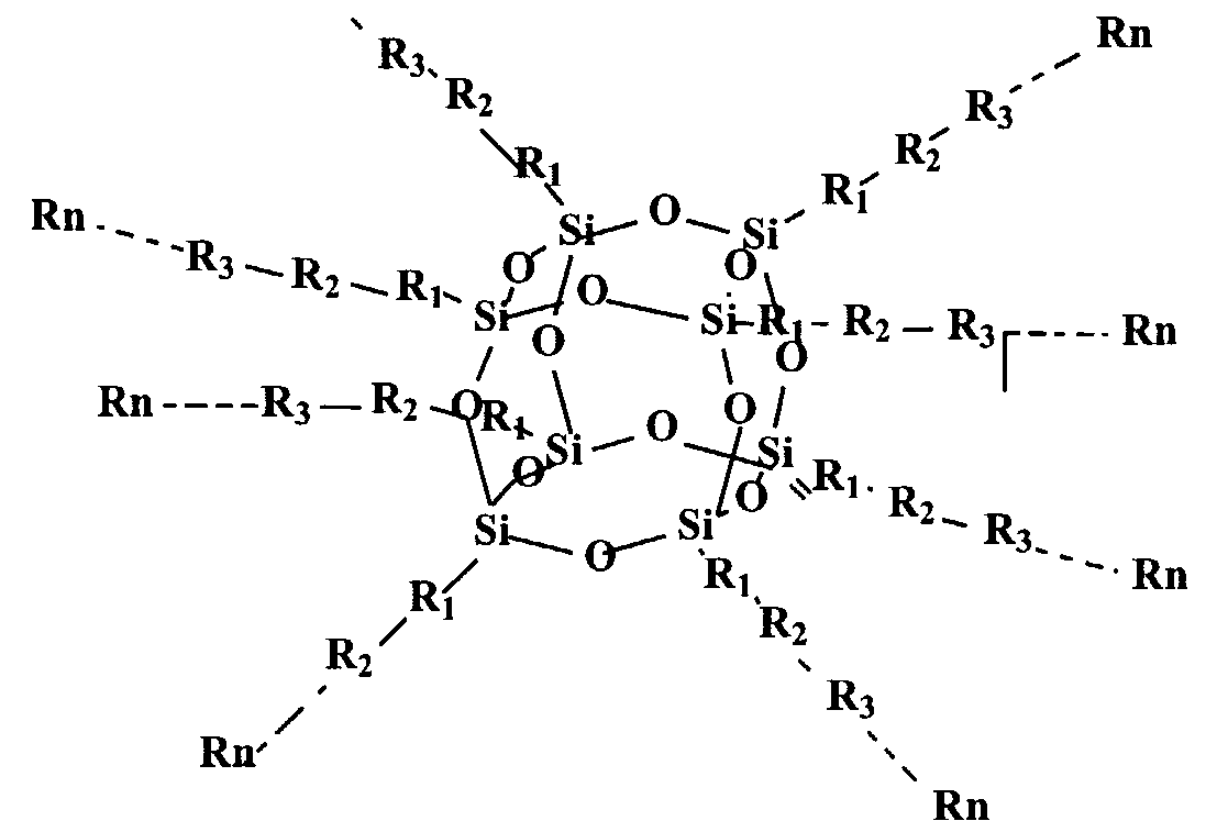
In a preferred embodiment of the above aspect of the invention, the compound may have the structural formula:
Rn
Figure imgf000014_0001
wherein R1 , R2...Rn can consist of aromatic ring structures and multi aromatic ring structures arranged so that a structure of low energy band gap is located either between the inner core and a structure of higher energy band gap, or between two such structures of higher energy band gap. These aromatic ring structures may be selected from the group consisting of phenyl, substituted phenyl, vinyl phenyl, substituted vinyl phenyl, arylene, heteroarylene, fused ring arylene, fused ring heteroarylene, alkoxy, alkylene, vinylene, ethynyl, and combinations thereof. The aromatic ring structures may be substituted by one or more functional groups, including electron-donating groups, electron-withdrawing groups, solubilising groups, silicon containing groups, metal containing groups, or Group III to V element containing groups or epoxy. The aromatic ring structures specifically include substituted phenyl wherein the phenyl substituents are selected from the group consisting of hydrogen, fluorine, chlorine, bromine, amino, alkoxy and alkylene.
Accordingly, a preferred embodiment of the above aspect of the invention relates to a hybrid light-emitting device material having a core structure and multiple surrounding layers, wherein the core structure is based on silsesquioxane architectures. The multiple layers may be formed of the same or different organic materials which are selected for their ability to provide one or more of the following effects, quantum confinement, improved solubility, suitable energy band gap for energy transfer, photoluminescence or electron luminescence, and spacer function of separation of different layers or functions.
The core structure of silsesquioxane material has the general formula (RSiO-ι.5)n wherein n typically ranges from 6 to 12 for discrete cage structures. More preferably n=8. Ri is selected either as the first layer or the part of the first layer having at least one function of providing the possibility of growing the second layer.
The above multi-layered quantum dot compound can be synthesized from a series of core polyhedral silsesquioxane intermediates having a variety of reactive substituent groups to provide the starting point of subsequent growth of multiple layers. Examples of typical reactive substituent groups of silsesquioxane intermediates include, but are not limited to, hydrogen, vinyl, phenyl, substituted phenyl, where the phenyl substituents include halo, amino, hydroxyl, vinyl, unsaturated alkyl, haloalkyl, silyl, etc. The core-multiple-layer structure can be realized either via layer by layer additions to the core structure or a one step reaction combining core and pre-prepared multiple layer components. One such organic quantum dot material having an octahedral silsesquioxane structure has the structure set out above, namely: Rn
Figure imgf000016_0001
wherein R1 , R2, R3,KRn are the multiple layer components which can be any group, such as, but not limited to, aromatic ring or multi-aromatic ring, the aromatic ring may be selected from the group consisting of arylene, heteroarylene, fused-ring arylene and fused-ring heteroarylene, alkoxy, alkylene, vinylene, ethynyl, and combinations of above moieties. The above moieties can be substituted by one or more functional groups such as electron-donating or electron-withdrawing groups, solubilising groups, silicon containing, metal containing, or lll-V element containing moieties, and epoxy. As will be appreciated, the additional functional groups chosen will depend upon the particular purpose for which the compound is intended to be used. Accordingly, in certain circumstances, other functional groups, having other desired properties, may be used. For this reason, the above specified functional groups should not be regarded as a closed list. Other groups could be used without departing from the nature and scope of this invention.
The above components can be synthesized from a series of core polyhedral selsequioxane intermediates having a variety of reactive substituent groups to provide the starting points of subsequent growth of multiple layers. For instance, typical reactive substituent groups of silsequioxane intermediates include, but are not limited to, hydrogen, vinyl and substituted phenyl. The phenyl subsituents may include halo, amino, hydroxyl, vinyl, unsaturated alkyl, haloalkyl, silyl etc.
The components (e.g. the core-multiple layer structures) can be synthesized by multiple reactions, adding the layers to the core one at a time, or by a one-step reaction which combines the core with pre-prepared multi functional group components, such as polymers.
In one preferred form of the invention, the inner core is formed of a cubic polyhedral digomeric silsesquioxand (POSS) structure. In this embodiment, the substituents are added to the inner core by grafting the eight corners of the POSS structure with oligo poly-phenylene or oligo poly-thiophene (e.g. POSS-2Ph, POSS-3Ph, POSS-4PH and POSS-Ph-2Th). The size of the quantum dot increases with increase in the number of phenyls or thiophenes grafted onto the structure. When the quantum dot size is smaller than the Bohr radius of the bulk exciton (which is generally about 2nm for organic semiconductor materials), the electronic excitation is strongly confined in all 3 dimensions. This collapses the continuous density of state of the bulk solid into discrete electronic states of the dot. Decreasing the dot diameter leads to large band gap energy and a blue shift in UV absorption spectra. Similarly, there tends to be a blue shift in photoluminescence as the quantum dot size decreases. These shifts in UV absorption and photoluminescence, with changing quantum dot size, confirms the quantum confined effect of such organic quantum dot systems. The quantum efficiencies of such quantum confined organic quantum dots are quite high - typically between about 25% and 45%.
It has been found that the colour of the quantum dot emission can be controlled both by manipulating the quantum dot size and by using different band gap materials. For example, if the oligo polyphenylene is substituted with oligo polythiophene (which has a lower band gap energy), the UV absorption and the photoluminescence spectra undergo a red shift to longer wavelength. Similarly, for POSS-3Ph, the photoluminescence peak is at about 380nm, whereas for POSS-Ph-2Thio, the photoluminescence peak is at about 500nm.
The compounds of a preferred embodiment of this invention can be considered as being 3-layered structures comprising an inner core (such as a polyhedral silsequioxane structure), a middle layer of oligo-conjugated polymers and an outer layer of alkyl chains. The energy band gap of the relevant oligo- conjugated polymers is less than that of both the inner core and the relevant alkyl chains. The electrons are thereby confined between the inner core and the outer alkyl chains. The compounds of this invention are able to be formed having particular particle sizes, quantum confinement in 3 dimensions, thermal stability, high photoluminescent quantum efficiencies, stable electroluminescent omissions, non-aggregation of particles and narrow emission widths. The methods of synthesizing these compounds are relatively straightforward. Also, the compounds can be tailored to have certain desired properties by modifying or varying the structure of the compounds. Accordingly, the compounds facilitate colour-tuneability and property tailorability of the devices made from them. Therefore, the compounds of the present invention have great potential in the field of semiconductor technology and other fields, including electroluminescent devices and diode lasers, wherein these materials can be used as emission materials or charge carrier transporting materials. Furthermore the compounds of this invention can be used as host or guest materials for energy transfer or quantum confinement for other materials. They also have applications in photovoltaic cells and as biosensors and biodetectors (e.g. fluorescent biological labels).
Throughout this specification, unless the context requires otherwise, the word "comprise" or variations such as "comprises" or "comprising", will be understood to imply the inclusion of a stated element, integer or step, or group of elements, integers or steps, but not the exclusion of any other element, integer or step, or group of elements, integers or steps.
Any discussion of documents, acts, materials, devices, articles or the like, which has been included in the present specification, is solely for the purpose of providing a context for the present invention. It is not to be taken as an admission that any or all of these matters form part of the prior art base or were common general knowledge in the field relevant to the present invention as it existed before the priority date of each claim of this application.
Description of the Drawings In order that the invention may be better understood, preferred forms will be illustrated by reference to the following drawings:
Figure 1 is a graph showing photoluminescence of a compound 4 thin film and dilute solution in the THF. Figure 2 is a graph showing photoluminescence of compound 5 thin film and dilute solution in the THF.
Figure 3 is a graph showing photoluminescence of blending a conventional polymer (having a higher band gap than compound 5) with compound 5 in thin film.
Figure 4 is a graph showing current against voltage in respect of a double layer electroluminescent device ITO/HTL/3a/Ca.
Figure 5 is a graph showing time resolved photoluminescence for a film of compound 5, a film in matrix (1 :3wt) and a dilute solution in THF.
Detailed Description of the Preferred Embodiments
In a preferred embodiment of this invention, the core structure is based on polyhedral octameric or cubic silsesquioxanes. Such a structure can represent building blocks from which subsequent reaction can add multiple layers one by one with desired properties or functions on each layer. The core structures are easily prepared in high yields from low cost starting materials which are commercially available. This rigid framework offers many appealing properties. Not only does it provide the crucial core structure with eight or more starting points to enable growth into a sphere-like quantum dot material, but it also enables development of unique models of silica surfaces which have special advantages in semiconductors. In the above structural formula, Ri is preferably hydrogen, phenyl, substituted phenyl or vinyl, wherein the phenyl substituents include halo, amino, hydroxyl, vinyl, unstaturated alkyl, haloalkyl, silyl, etc.
As mentioned above, the organic quantum dot materials can be synthesized from polyhedral silsesquioxane intermediates having reactive substituent groups capable of reacting with other functional groups to form either the core-multiple-layers or core-first-layer structures followed by subsequent reactions adding layers one by one. Several possible reactions that can be used for this purpose are illustrated generally below. Such reactions include, but are not limited to, metal catalyzed hydrosilation, Gragnard reaction, Heck reaction, Suzuki coupling reaction, and Buchwald Hartwig amination.
The multiple layers have a variety of functions or results, including but not limited to, quantum confinement, improved solubility, matching of energy band gap for energy transfer, photoluminescence or electroluminescence, electron or hole transporting or injection, isolation of different layers or functions, etc. The components of each layer can be selected from conventional structures with desired properties. For example, the emissive layer can be formed of any arylene, heteroarylene, fused-ring arylene and fused-ring heteroarylene. The solubilising or quantum confinement layer and spacer can be formed of any of alkoxy, alkylene, or single atom such as S, O, N, Si, metal, etc.
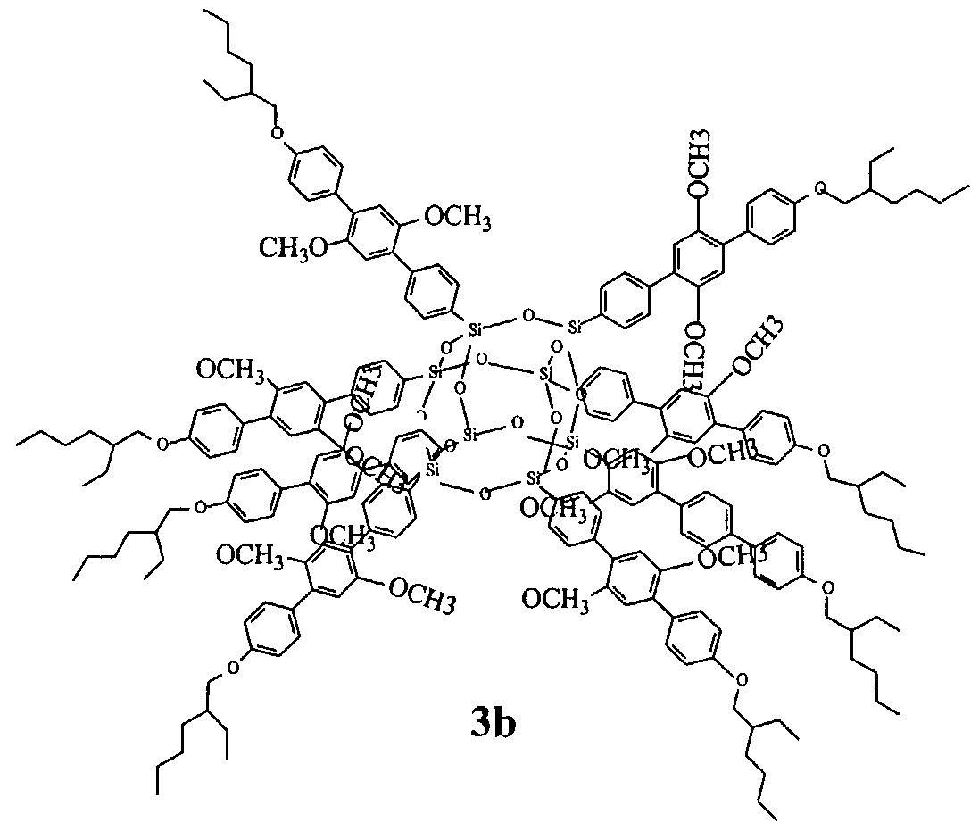
Some example structures of compounds of the present invention are:
Figure imgf000020_0001
Figure imgf000020_0002
Figure imgf000021_0001
Figure imgf000021_0002
Figure imgf000021_0003
Figure imgf000022_0001
Turning to the drawings, the graph of Figure 1 contains 2 curves showing the photoluminescence of compound 4 both in solution and as a film. The graph of Figure 2 also contains 2 curves which represent the photoluminescence of compound 5, both in solution and as a film. As can be seen, the well matched PL spectra of the solution and the film in each case indicates that there is no significant aggregation of the compound in the solid state. For conventional polymers and oligomers, there is a common phenomenon of PL spectra red shifts of film over solution due to aggregation of the compounds in their solid states. This lack of aggregation is a substantial benefit of the compounds of the present invention.
In a blending system there is an effective energy transfer from higher band gap environment (polymer) to a material, such as one of the new compounds, having a lower band gap. Figure 3 shows a blending system in which there is an effective energy transfer from the higher band gap material (ie a polymer) to the material of compound 5 which has lower band gap than the polymer. The PL peak of compound 5 (486nm) remains unchanged as polymer content increases and PL quantum gets higher. This demonstrates the intrinsic three dimensional quantum confinement exhibited by compound 5. Materials without intrinsic quantum confinement will have their PL peak blue shift as blending with higher band gap materials occurs. This is because the higher band gap surrounding material will help lower band gap molecules separate from each other causing their excitons to become more and more localized.
Figure 4 is a graph showing the change in current/luminescence as the voltage increases across a double layer device formed of ITO/HTL/3a/Ca (where 3a is the compound 3a referred to above). This graph shows the preliminary results of the double layer electroluminescent device. The substantial delay in the increase of luminescence compared to the current suggests that the electron injection and transporting are the crucial step. Consequently, better performance is expected if an ETL (electron transporting layer) is added between the cathode and compound 3a. This indicates that the materials can be used as emissive candidates.
Figure 5 is a graph showing time resolved photoluminescence of a film of the compound 5, a film in matrix of compound 4 (1 :3 wt), and a dilute solution in THF. As can be seen, the photoluminescent decay of the solution, the film in matrix (higher band gap material), and the film all have similar decay times (150ps-180ps). This suggests that the carriers are localized even in the film sample, again demonstrating the intrinsic quantum confinement in compound 5. Conventional polymers normally show a big difference in photoluminescence depending on whether they are in the form of a film (e.g. about 100ps) or a solution (e.g. about 1000ps).
Preferred embodiments of the invention are exemplified below.
Example 1 :
Compound 1 can be formulated as shown below:
Figure imgf000024_0001
Bromine (7.2g, 45mmol) was added dropwise to a suspension containing phenylsilsesquioxane (5.16g, 5mmol) and ferric chloride (0.4g, 2.4mmol) in 300ml chloroform. After stirring for 96 hrs at room temperature, the solution was poured into a saturated sodium carbonate water solution 2000ml. The water phase was washed with 400ml chloroform two times and all the organic phases were combined together and washed with 400ml water. The organic phase was filtered through a 0.45um syringe filter and the solvent was removed from the filtrate. A white crystal of compound 1 (4.9g, 60%) was obtained by adding methanol and filtering out the methanol. Proton NMR indicated that there was no starting material remaining and this is consistent with the expected structure. 29Si NMR
(solid): -69.8, 70.9, -74.2. GPC showed only one sharp peak and polydispersity index of 1.02 which means there are no polymers present. The results are shown in Table 1 , together with the results of the other examples (see below). Example 2:
Compound 3 can be formulated as shown below:
Figure imgf000025_0001
Following Gragnard reaction procedures, compound A (4.67g, 12mmol) in 30ml dry THF was added dropwise into a RBF containing 0.302g Mg under Argon and refluxing. After 8 hrs the solution was cooled to room temperature and transferred to another RBF (under Argon) which contained compound 1 and catalyst tetrakis(triphenyl-phosphine)palladium(0) resolved in 10ml dry THF under stirring. The solution was then refluxed for 24 hrs and the reaction mixture was then cooled to room temperature. Saturated NH4CI solution was then added into the RBF and the organic phase was then extracted. The compound 3 (1.9g, 54%) was obtained as white crystals through silica gel column chromatography purification. GPC indicated that there is only one sharp peak with polydispersity index of 1.03. 29Si NMR (CDCI3): -69.2, -69.8, -70.5. XRD indicated that the compound 3 has uniform size that corresponds with theoretical calculations. The results are again summarised in Table 1. DSC revealed there is no Tg. Photoluminescent emission is 386nm for the compound as a thin film and 388nm for the compound as a dilute solution, both of them giving off bright blue light. Absolute quantum efficiency (integrating sphere) giving a photoluminescent efficiency above 30% was achieved for the thin film (as summarized in Table 1 ).
Example 3:
Compound 2 can be formulated as shown below:
Figure imgf000026_0001
Compound 2 was obtained, through the reaction exemplified above, by reacting compounds 1 and B. The same procedures were followed as in Example 2 to give a white solid in a yield of about 60%. GPC indicated that there is only one sharp peak with polydispersity index of 1.02. XRD indicated that the compound 2 has uniform size that corresponds with theoretical calculations. DSC revealed there is no Tg. Photoluminescent emission is 368nm for the compound as a thin film and 366nm for it as a dilute solution, both of them giving off bright blue light. Absolute quantum efficiency (integrating sphere) giving a photoluminescent efficiency of above 25% was achieved for the thin film.- Again, the above results are summarized in Table 1.
Example 4:
Compound 4 can be formulated as shown below:
Figure imgf000026_0002
Butyllithium (1.2M in hexane) (2.6ml) was added dropwise into a solution of compound C (1.0962g, 2.357mmol 0.4M in dry THF) at -78°C under Argon and stirring. After 1 hr, a solution, prepared by BrCH2CH2Br (0.8648g, 4.6mmol) and
Mg (0.1159g, 4.83mmol) reacted in room temperature for 30mins, was transferred to the reaction mixture under stirring and gradually the temperature was increased to room temperature. After 2 hrs the whole mixture was transferred to a RBF which contained compound 1 (0.3047g, 0.1755mmol) and catalyst tetrakis(triphenyl-phosphine)palladium(0) under Argon. This mixture was then refluxed for 24hrs and the organic phase was extracted following the same procedures as performed in Example 2. After purification by a silica gel column a white crystal of compound 4 (0.156, 21 %) was obtained. GPC indicated that there is only one sharp peak with polydispersity index of 1.03. 29Si NMR (CDCI3):
-69.35. XRD indicated that the compound 4 has uniform size that corresponds with theoretical calculations. DSC revealed there is no Tg. Photoluminescent emission is 380nm for the thin film and 387nm for dilute solution, both of them giving off bright blue light. Absolute quantum efficiency (integrating sphere) giving a photoluminescent efficiency of about 40% for the thin film was achieved. The results are again summarised in Table 1.
Example 5:
Compound 5 can be formulated as shown below:
Figure imgf000027_0001
Compound 5 was obtained through the above reaction by reacting compounds 1 and D, following the same procedures in Example 2 to give a green solid in yield 35%. Photoluminescent emission is 486nm for thin film and dilute solution, both of them giving off bright green light. Time-resolved Photoluminescent analysis for thin film and dilute solution revealed the decay time of excitons are almost the same in both cases. The similar result was obtained from a matrix system by blending compound 4 (having a higher band gap) with compound 5. This provides strong evidence demonstrating the quantum confinement, even in solid state, of compound 5. See Figure 5.
Table 1: Particle size by XRD and Mw by GPC
Figure imgf000028_0001
Table 1 shows the results of analyses performed on the compounds produced in the Examples. For instance, Table 1 shows the particle sizes of the compounds, determined from wide-angle XRD, compared with the size of the compounds determined by theoretical calculations. The Table also shows the compounds' molecular weights (g/mol) from GPC and absolute photoluminescent quantum efficiencies (PLQE) from the integrating sphere.
Table 2: Time resolved Photoluminescent for 2, 3, 4 of dilute solution in THF
Figure imgf000028_0002
Table 2 shows the time resolved photoluminescence for dilute solutions of compounds 2, 3 and 4 in THF. The increase of decay time with molecular size, together with the increase of emission wavelength, indicates the presence of quantum confinement effects.
It will be appreciated by persons skilled in the art that numerous variations and/or modifications may by made to the invention as described herein without departing from the spirit or scope of the invention. The present embodiments are therefore to be considered in all respects as illustrative and not restrictive.

Claims

CLAIMS:The claims defining this invention are as follows:
1. A quantum dot semiconductor compound comprising an inner core adapted to have 3 or more substituents attached thereto, wherein at least one of the substituents includes an organic functional moiety adapted to exhibit three dimensional quantum confinement.
2. A compound according to claim 1 wherein the inner core is formed of carbon, silicon, or a polyhedral silsesquioxane structure.
3. A compound according to claim 2 wherein the inner core is formed of a polyhedral silsesquioxane structure.
4. A compound according to claim 3 wherein the polyhedral silsesquioxane has a general formula of (SiOι.5)n, wherein n ranges from 6 to 100.
5. A compound according to claim 4 wherein n ranges from 6 to 12.
6. A compound according to claim 5 wherein the silsesquioxane structure is an octahedral or cubic structure.
7. A compound according to claim 6 wherein the silsesquioxane structure has up to 8 substituents attached thereto, each of which includes at least one of said organic functional moieties.
8. A compound according to any one of claims 1 to 7 wherein one organic functional moiety of each substituent is attached to the inner core and the energy band gap of the organic functional moiety is less than the energy band gap of the inner core.
9. A compound according to claim 8 wherein each organic functional moiety has an additional functional group attached thereto, and each such functional group has an energy band gap higher than the energy band gap of the organic functional moiety to which it is attached.
10. A compound according to claim 9 wherein each additional functional group has a further functional group attached thereto.
1 1 . A compound according to any one of claims 7 to 10 wherein each said substituent consists of 2 or more of said organic functional moieties.
12 A compound according to claim 1 1 wherein the 2 or more moieties are attached together in blocks. 13. A compound according to claim 11 or claim 12 wherein the organic functional moieties are located in blocks of one or more moieties, separated by one or more additional functional groups, said functional groups having a higher energy band gap than said moieties.
14 A compound according to any one of claims 7 to 13 wherein the organic functional moieties are the same. 15. A compound according to any one of claims 7 to 13 wherein the organic functional moieties are not all the same.
16. A compound according to any one of claims 1 to 15 wherein a terminal end of each substituent comprises an alkyl chain.
17. A compound according to claim 9, claim 10 or claim 16 wherein the additional functional group, the further functional group or the alkyl chain are selected from groups which confer on the compound desired properties selected from quantum confinement, improved solubility, hole transport, electron transport, electroluminescent, and photoluminescent properties.
18. A compound according to any one of claims 1 to 7 wherein each substituent comprises a polymer and the organic functional moiety forms part of the polymer.
19. A compound according to claim 18 wherein the organic functional moiety is connected to the inner core and the energy band gap of the organic functional moiety is lower than that of both the inner core and a monomeric unit adjoining the organic functional moiety.
20. A compound according to claim 18 wherein each polymer comprises 2 or more of said organic functional moieties.
21. A compound according to claim 20 wherein the 2 or more moieties are attached together in blocks. 22. A compound according to claim 18 wherein the polymer comprises one organic functional moiety and said moiety is positioned between 2 monomeric units of the polymer, both of which have energy band gaps higher than that of the organic functional moiety.
23. A compound according to claim 21 wherein the blocks of 2 or more of said moieties are positioned between 2 monomeric units of the polymer, both of which have energy band gaps higher than that of said moieties.
24. A compound according to any one of claims 18 to 23 wherein the polymers are oligo-conjugated polymers.
25. A compound according to claim 24 wherein the polymers include oligo- polyphenylene or oligo polythiophene.
26. A compound according to any one of claims 1 to 25 wherein all of the substituents include one of said organic functional moieties attached to the inner core, said functional moieties forming a first layer shell about said inner core.
27. A compound according to claim 26 wherein all of the substituents include one of said additional functional groups attached to the organic functional moiety, forming a second layer shell about said inner core. 28. A compound according to claim 27 wherein each additional functional group is a polymer.
29. A compound according to claim 28 wherein each polymer is an oligo- conjugated polymer.
30. A compound according to any one of claims 27 to 29 wherein all of the substituents include one of said further functional groups attached to the additional functional group, forming a third layer shell about said inner core.
31. A compound according to claim 30 wherein the further functional group is an alkyl chain.
32. A compound according to any one of claims 26 to 31 wherein the inner core is a polyhedral silsesquioxane structure having from 6 to 12 substituents attached thereto.
33. A compound according to claim 32 wherein the polyhedral silsesquioxane structure has substituents selected from the group consisting of: an organic functional moiety adapted to exhibit three dimensional quantum confinement; such an organic functional moiety having a functional group attached thereto, said organic functional moiety having a lower energy band gap than the functional group; a functional group having such a functional moiety attached thereto, said functional group having a higher energy band gap than the organic functional moiety; and a polymer which includes such an organic functional moiety, wherein any monomeric unit which adjoins the organic functional moiety has a higher energy band gap than the organic functional moiety.
34. A compound according to claim 33 wherein each substituent comprises said polymer.
35. A compound according to claim 34 wherein the polymer is an oligo- conjugated polymer. 36. A compound according to claim 34 or claim 35 wherein said polymer includes an alkyl chain attached thereto.
37. A compound according to any one of claims 34 to 36 wherein the polymer comprises one organic functional moiety and said moiety is positioned between 2 monomeric units of the polymer, both of which have energy band gaps higher than that of the organic functional moiety.
38. A compound according to any one of claims 34 to 36 wherein the polymer comprises 2 or more of said organic functional moieties.
39. A compound according to claim 38 wherein the 2 or more moieties are attached together in blocks. 40. A compound according to claim 39 wherein the blocks of 2 or more of said moieties are positioned between 2 monomeric units of the polymer, both of which units have energy band gaps higher than that of said moieties. 41. A compound according to claim 34 having the structural formula:
Rn
Figure imgf000033_0001
wherein R1 , R2...Rn are selected from the group consisting of aromatic ring structures and multi aromatic ring structures. 42. A compound according to claim 41 wherein said aromatic ring structures are selected from the group consisting of phenyl, substituted phenyl, vinyl phenyl, substituted vinyl phenyl, arylene, heteroarylene, fused ring arylene, fused ring heteroarylene, alkoxy, alkylene, vinylene, ethynyl, and combinations thereof.
43. A compound according to claim 42 wherein said aromatic ring structures are substituted by one or more functional groups, including electron- donating groups, electron-withdrawing groups, solubilising groups, silicon containing groups, metal containing groups, or Group III to V element containing groups or epoxy.
44. A compound according to claim 42 wherein the aromatic ring structures include substituted phenyl and the phenyl substituents are selected from the group consisting of hydrogen, fluorine, chlorine, bromine, amino, alkoxy and alkylene.
45. A quantum dot semiconductor compound selected from the following:
Figure imgf000034_0001
Figure imgf000034_0002
Figure imgf000035_0001
Figure imgf000036_0001
6. A quantum dot semiconductor compound substantially as hereinbefore defined with reference to any one of Figures 1 to 5 and any one of the examples.
PCT/SG2004/000004 2003-01-06 2004-01-06 Quantum confined light-emitting dot material for low dimensional semiconductors WO2004060898A1 (en)

Applications Claiming Priority (2)

Application Number Priority Date Filing Date Title
SG200300030A SG115513A1 (en) 2003-01-06 2003-01-06 Quantum confined light-emitting dot material for low dimensional semiconductors
SG200300030-4 2003-01-06

Publications (2)

Publication Number Publication Date
WO2004060898A1 true WO2004060898A1 (en) 2004-07-22
WO2004060898A8 WO2004060898A8 (en) 2004-10-21

Family

ID=32710087

Family Applications (1)

Application Number Title Priority Date Filing Date
PCT/SG2004/000004 WO2004060898A1 (en) 2003-01-06 2004-01-06 Quantum confined light-emitting dot material for low dimensional semiconductors

Country Status (2)

Country Link
SG (1) SG115513A1 (en)
WO (1) WO2004060898A1 (en)

Cited By (4)

* Cited by examiner, † Cited by third party
Publication number Priority date Publication date Assignee Title
WO2009006550A1 (en) * 2007-07-05 2009-01-08 Nitto Denko Corporation Light emitting devices and compositions
WO2010045263A2 (en) * 2008-10-13 2010-04-22 Nitto Denko Corporation Printable light-emitting compositions
US7993747B2 (en) 2006-05-15 2011-08-09 Nitto Denko Corporation Light emitting devices and compositions comprising lumophore-functionalized nanoparticles
US8597803B2 (en) 2007-11-15 2013-12-03 Nitto Denko Corporation Light emitting devices and compositions

Citations (6)

* Cited by examiner, † Cited by third party
Publication number Priority date Publication date Assignee Title
US5939576A (en) * 1998-01-05 1999-08-17 The United States Of America As Represented By The Secretary Of The Air Force Method of functionalizing polycyclic silicones and the compounds so formed
US5942638A (en) * 1998-01-05 1999-08-24 The United States Of America As Represented By The Secretary Of The Air Force Method of functionalizing polycyclic silicones and the resulting compounds
US6100417A (en) * 1999-08-31 2000-08-08 The United States Of America As Represented By The Secretary Of The Air Force Functionalizing olefin bearing silsesquioxanes
WO2002005971A1 (en) * 2000-07-14 2002-01-24 Canon Kabushiki Kaisha Organic-inorganic hybrid light emitting devices (hled)
WO2002100867A1 (en) * 2000-10-27 2002-12-19 The Regents Of The University Of Michigan Well-defined nanosized building blocks for organic/inorganic nanocomposites
US20030105246A1 (en) * 2001-11-05 2003-06-05 Hideki Andoh Silicone resin compositions and molded products of silicone resins

Patent Citations (6)

* Cited by examiner, † Cited by third party
Publication number Priority date Publication date Assignee Title
US5939576A (en) * 1998-01-05 1999-08-17 The United States Of America As Represented By The Secretary Of The Air Force Method of functionalizing polycyclic silicones and the compounds so formed
US5942638A (en) * 1998-01-05 1999-08-24 The United States Of America As Represented By The Secretary Of The Air Force Method of functionalizing polycyclic silicones and the resulting compounds
US6100417A (en) * 1999-08-31 2000-08-08 The United States Of America As Represented By The Secretary Of The Air Force Functionalizing olefin bearing silsesquioxanes
WO2002005971A1 (en) * 2000-07-14 2002-01-24 Canon Kabushiki Kaisha Organic-inorganic hybrid light emitting devices (hled)
WO2002100867A1 (en) * 2000-10-27 2002-12-19 The Regents Of The University Of Michigan Well-defined nanosized building blocks for organic/inorganic nanocomposites
US20030105246A1 (en) * 2001-11-05 2003-06-05 Hideki Andoh Silicone resin compositions and molded products of silicone resins

Non-Patent Citations (6)

* Cited by examiner, † Cited by third party
Title
BAKER ET AL: "3-Dimensional structural chracterization of cationized polyhedral oligomeric silsesquixones (POSS) with styrl and phenylethyl capping agents", INT J MASS SPECTROMETRY, vol. 227, 2003, pages 205 - 216 *
BASSINDALE ET AL: "Fluoride-ion encapsulation within a silsesquioxane cage", ANGEW CHEM INT, vol. 42, 2003, pages 3488 - 3490 *
CHOI ET AL: "Organic/inorganic nanocomposites from silsesquioxane", POLYMERIC MATERIALS: SCIENCE AND ENGINEERING, vol. 84, 2001, pages 735 *
FEHER ET AL: "Phosphine-substituted silsesquioxanes as building blocks for organometallic gels", ORGANOMETALLICS, vol. 14, 1995, pages 4452 - 4453 *
HARRISON ET AL: "Porous materials from trigonal-prismatic {Si6O9} and {Si8O12} cage monomers", CHEM COMM, 1996, pages 415 - 416 *
LIN ET AL: "Theoretical studies in monosubstituted and higher phenyl-substituted octahydrosilsesquioxanes", J PHYS CHEM B, vol. 107, 2003, pages 13788 - 13792 *

Cited By (7)

* Cited by examiner, † Cited by third party
Publication number Priority date Publication date Assignee Title
US7993747B2 (en) 2006-05-15 2011-08-09 Nitto Denko Corporation Light emitting devices and compositions comprising lumophore-functionalized nanoparticles
WO2009006550A1 (en) * 2007-07-05 2009-01-08 Nitto Denko Corporation Light emitting devices and compositions
US8609258B2 (en) 2007-07-05 2013-12-17 Nitto Denko Corporation Light emitting devices and compositions
US8597803B2 (en) 2007-11-15 2013-12-03 Nitto Denko Corporation Light emitting devices and compositions
WO2010045263A2 (en) * 2008-10-13 2010-04-22 Nitto Denko Corporation Printable light-emitting compositions
WO2010045263A3 (en) * 2008-10-13 2010-07-08 Nitto Denko Corporation Printable light-emitting compositions
US8721922B2 (en) 2008-10-13 2014-05-13 Nitto Denko Corporation Printable light-emitting compositions

Also Published As

Publication number Publication date
WO2004060898A8 (en) 2004-10-21
SG115513A1 (en) 2005-10-28

Similar Documents

Publication Publication Date Title
US10770619B2 (en) Light-emitting devices and displays with improved performance
Skaff et al. Quantum Dots Tailored with Poly (p ara-phenylene vinylene)
Huang et al. Polyhedral oligomeric silsesquioxane enhances the brightness of perovskite nanocrystal-based green light-emitting devices
KR102259782B1 (en) Metal halide perovskite light-emitting diode and preparation method thereof
Wei et al. Homogeneous synthesis and electroluminescence device of highly luminescent CsPbBr3 perovskite nanocrystals
US20060128845A1 (en) Quantum dots tailored with electronically-active polymers
US20100051901A1 (en) Light emitting devices and displays with improved performance
US7794856B2 (en) Organic light-emitting device and display apparatus
Bae et al. Reduced efficiency roll-off in light-emitting diodes enabled by quantum dot–conducting polymer nanohybrids
US11091690B2 (en) Quantum dots, a composition or composite including the same, and an electronic device including the same
KR20210077111A (en) Defect suppressed metal halide perovskite light-emitting material and light-emitting diode comprising the same
Wang et al. Quantum dot light-emitting diode using solution-processable graphene oxide as the anode interfacial layer
KR20210056275A (en) Quantum dots and composite and display device including the same
Xu et al. Ultrasonication-assisted ambient-air synthesis of monodispersed blue-emitting CsPbBr3 quantum dots for white light emission
Xu et al. A new star-shaped carbazole derivative with polyhedral oligomeric silsesquioxane core: Crystal structure and unique photoluminescence property
Xin et al. Highly emissive and color-tunable perovskite cross-linkers for luminescent polymer networks
DE102004040005A1 (en) Transition metal carbene complexes embedded in polymer matrices for use in OLEDs
Kunz et al. Photo-cross-linkable polymer inks for solution-based OLED fabrication
CN110114701B (en) Light-emitting resin composition for wavelength conversion, method for producing same, wavelength conversion member, and light-emitting element
Jo et al. Solution-processed fabrication of light-emitting diodes using CsPbBr3 perovskite nanocrystals
Fu et al. Engineering of annealing and surface passivation toward efficient and stable quasi-2d perovskite light-emitting diodes
Liu et al. A comparative study on luminescent copolymers of fluorene and carbazole with conjugated or δ-Si interrupted structures: steric effects
WO2004060898A1 (en) Quantum confined light-emitting dot material for low dimensional semiconductors
Dong et al. Constructing Perovskite/Polymer Core/Shell Nanocrystals with Simultaneous High Efficiency and Stability for Mini-LED Backlights
KR20210049702A (en) Core shell quantum dot and electronic device including the same

Legal Events

Date Code Title Description
AK Designated states

Kind code of ref document: A1

Designated state(s): AE AG AL AM AT AU AZ BA BB BG BR BW BY BZ CA CH CN CO CR CU CZ DE DK DM DZ EC EE EG ES FI GB GD GE GH GM HR HU ID IL IN IS JP KE KG KP KR KZ LC LK LR LS LT LU LV MA MD MG MK MN MW MX MZ NA NI NO NZ OM PG PH PL PT RO RU SC SD SE SK SL SY TJ TM TN TR TT TZ UA UG US UZ VC VN YU ZA ZM ZW

AL Designated countries for regional patents

Kind code of ref document: A1

Designated state(s): BW GH GM KE LS MW MZ SD SL SZ TZ UG ZM ZW AM AZ BY KG KZ MD RU TJ TM AT BE BG CH CY CZ DE DK EE ES FI FR GB GR HU IE IT LU MC NL PT RO SE SI SK TR BF BJ CF CG CI CM GA GN GQ GW ML MR NE SN TD TG

CFP Corrected version of a pamphlet front page
CR1 Correction of entry in section i

Free format text: IN PCT GAZETTE 30/2004 ADD "DECLARATION UNDER RULE 4.17: - AS TO APPLICANT S ENTITLEMENT TO APPLY FOR AND BE GRANTED A PATENT (RULE 4.17(II))."; ADD "DECLARATION UNDER RULE 4.17: - AS TO THE APPLICANT S ENTITLEMENT TO CLAIM THE PRIORITY OF THE EARLIER APPLICATION (RULE 4.17(III)) FOR ALL DESIGNATIONS."

121 Ep: the epo has been informed by wipo that ep was designated in this application
122 Ep: pct application non-entry in european phase
DPEN Request for preliminary examination filed prior to expiration of 19th month from priority date (pct application filed from 20040101)