WO2006103874A1 - Organic electroluminescent device material, organic electroluminescent device, display and illuminating device - Google Patents
Organic electroluminescent device material, organic electroluminescent device, display and illuminating device Download PDFInfo
- Publication number
- WO2006103874A1 WO2006103874A1 PCT/JP2006/304234 JP2006304234W WO2006103874A1 WO 2006103874 A1 WO2006103874 A1 WO 2006103874A1 JP 2006304234 W JP2006304234 W JP 2006304234W WO 2006103874 A1 WO2006103874 A1 WO 2006103874A1
- Authority
- WO
- WIPO (PCT)
- Prior art keywords
- group
- substituent
- general formula
- organic
- partial structure
- Prior art date
Links
Classifications
-
- C—CHEMISTRY; METALLURGY
- C09—DYES; PAINTS; POLISHES; NATURAL RESINS; ADHESIVES; COMPOSITIONS NOT OTHERWISE PROVIDED FOR; APPLICATIONS OF MATERIALS NOT OTHERWISE PROVIDED FOR
- C09K—MATERIALS FOR MISCELLANEOUS APPLICATIONS, NOT PROVIDED FOR ELSEWHERE
- C09K11/00—Luminescent, e.g. electroluminescent, chemiluminescent materials
- C09K11/06—Luminescent, e.g. electroluminescent, chemiluminescent materials containing organic luminescent materials
-
- H—ELECTRICITY
- H05—ELECTRIC TECHNIQUES NOT OTHERWISE PROVIDED FOR
- H05B—ELECTRIC HEATING; ELECTRIC LIGHT SOURCES NOT OTHERWISE PROVIDED FOR; CIRCUIT ARRANGEMENTS FOR ELECTRIC LIGHT SOURCES, IN GENERAL
- H05B33/00—Electroluminescent light sources
- H05B33/12—Light sources with substantially two-dimensional radiating surfaces
- H05B33/14—Light sources with substantially two-dimensional radiating surfaces characterised by the chemical or physical composition or the arrangement of the electroluminescent material, or by the simultaneous addition of the electroluminescent material in or onto the light source
-
- H—ELECTRICITY
- H10—SEMICONDUCTOR DEVICES; ELECTRIC SOLID-STATE DEVICES NOT OTHERWISE PROVIDED FOR
- H10K—ORGANIC ELECTRIC SOLID-STATE DEVICES
- H10K85/00—Organic materials used in the body or electrodes of devices covered by this subclass
- H10K85/30—Coordination compounds
- H10K85/321—Metal complexes comprising a group IIIA element, e.g. Tris (8-hydroxyquinoline) gallium [Gaq3]
-
- H—ELECTRICITY
- H10—SEMICONDUCTOR DEVICES; ELECTRIC SOLID-STATE DEVICES NOT OTHERWISE PROVIDED FOR
- H10K—ORGANIC ELECTRIC SOLID-STATE DEVICES
- H10K85/00—Organic materials used in the body or electrodes of devices covered by this subclass
- H10K85/30—Coordination compounds
- H10K85/341—Transition metal complexes, e.g. Ru(II)polypyridine complexes
- H10K85/342—Transition metal complexes, e.g. Ru(II)polypyridine complexes comprising iridium
-
- C—CHEMISTRY; METALLURGY
- C09—DYES; PAINTS; POLISHES; NATURAL RESINS; ADHESIVES; COMPOSITIONS NOT OTHERWISE PROVIDED FOR; APPLICATIONS OF MATERIALS NOT OTHERWISE PROVIDED FOR
- C09K—MATERIALS FOR MISCELLANEOUS APPLICATIONS, NOT PROVIDED FOR ELSEWHERE
- C09K2211/00—Chemical nature of organic luminescent or tenebrescent compounds
- C09K2211/10—Non-macromolecular compounds
- C09K2211/1018—Heterocyclic compounds
- C09K2211/1025—Heterocyclic compounds characterised by ligands
- C09K2211/1029—Heterocyclic compounds characterised by ligands containing one nitrogen atom as the heteroatom
- C09K2211/1037—Heterocyclic compounds characterised by ligands containing one nitrogen atom as the heteroatom with sulfur
-
- C—CHEMISTRY; METALLURGY
- C09—DYES; PAINTS; POLISHES; NATURAL RESINS; ADHESIVES; COMPOSITIONS NOT OTHERWISE PROVIDED FOR; APPLICATIONS OF MATERIALS NOT OTHERWISE PROVIDED FOR
- C09K—MATERIALS FOR MISCELLANEOUS APPLICATIONS, NOT PROVIDED FOR ELSEWHERE
- C09K2211/00—Chemical nature of organic luminescent or tenebrescent compounds
- C09K2211/10—Non-macromolecular compounds
- C09K2211/1018—Heterocyclic compounds
- C09K2211/1025—Heterocyclic compounds characterised by ligands
- C09K2211/1044—Heterocyclic compounds characterised by ligands containing two nitrogen atoms as heteroatoms
-
- C—CHEMISTRY; METALLURGY
- C09—DYES; PAINTS; POLISHES; NATURAL RESINS; ADHESIVES; COMPOSITIONS NOT OTHERWISE PROVIDED FOR; APPLICATIONS OF MATERIALS NOT OTHERWISE PROVIDED FOR
- C09K—MATERIALS FOR MISCELLANEOUS APPLICATIONS, NOT PROVIDED FOR ELSEWHERE
- C09K2211/00—Chemical nature of organic luminescent or tenebrescent compounds
- C09K2211/10—Non-macromolecular compounds
- C09K2211/1018—Heterocyclic compounds
- C09K2211/1025—Heterocyclic compounds characterised by ligands
- C09K2211/1059—Heterocyclic compounds characterised by ligands containing three nitrogen atoms as heteroatoms
-
- C—CHEMISTRY; METALLURGY
- C09—DYES; PAINTS; POLISHES; NATURAL RESINS; ADHESIVES; COMPOSITIONS NOT OTHERWISE PROVIDED FOR; APPLICATIONS OF MATERIALS NOT OTHERWISE PROVIDED FOR
- C09K—MATERIALS FOR MISCELLANEOUS APPLICATIONS, NOT PROVIDED FOR ELSEWHERE
- C09K2211/00—Chemical nature of organic luminescent or tenebrescent compounds
- C09K2211/10—Non-macromolecular compounds
- C09K2211/1018—Heterocyclic compounds
- C09K2211/1025—Heterocyclic compounds characterised by ligands
- C09K2211/1074—Heterocyclic compounds characterised by ligands containing more than three nitrogen atoms as heteroatoms
-
- C—CHEMISTRY; METALLURGY
- C09—DYES; PAINTS; POLISHES; NATURAL RESINS; ADHESIVES; COMPOSITIONS NOT OTHERWISE PROVIDED FOR; APPLICATIONS OF MATERIALS NOT OTHERWISE PROVIDED FOR
- C09K—MATERIALS FOR MISCELLANEOUS APPLICATIONS, NOT PROVIDED FOR ELSEWHERE
- C09K2211/00—Chemical nature of organic luminescent or tenebrescent compounds
- C09K2211/10—Non-macromolecular compounds
- C09K2211/1018—Heterocyclic compounds
- C09K2211/1025—Heterocyclic compounds characterised by ligands
- C09K2211/1088—Heterocyclic compounds characterised by ligands containing oxygen as the only heteroatom
-
- C—CHEMISTRY; METALLURGY
- C09—DYES; PAINTS; POLISHES; NATURAL RESINS; ADHESIVES; COMPOSITIONS NOT OTHERWISE PROVIDED FOR; APPLICATIONS OF MATERIALS NOT OTHERWISE PROVIDED FOR
- C09K—MATERIALS FOR MISCELLANEOUS APPLICATIONS, NOT PROVIDED FOR ELSEWHERE
- C09K2211/00—Chemical nature of organic luminescent or tenebrescent compounds
- C09K2211/10—Non-macromolecular compounds
- C09K2211/1018—Heterocyclic compounds
- C09K2211/1025—Heterocyclic compounds characterised by ligands
- C09K2211/1092—Heterocyclic compounds characterised by ligands containing sulfur as the only heteroatom
-
- C—CHEMISTRY; METALLURGY
- C09—DYES; PAINTS; POLISHES; NATURAL RESINS; ADHESIVES; COMPOSITIONS NOT OTHERWISE PROVIDED FOR; APPLICATIONS OF MATERIALS NOT OTHERWISE PROVIDED FOR
- C09K—MATERIALS FOR MISCELLANEOUS APPLICATIONS, NOT PROVIDED FOR ELSEWHERE
- C09K2211/00—Chemical nature of organic luminescent or tenebrescent compounds
- C09K2211/18—Metal complexes
- C09K2211/185—Metal complexes of the platinum group, i.e. Os, Ir, Pt, Ru, Rh or Pd
-
- C—CHEMISTRY; METALLURGY
- C09—DYES; PAINTS; POLISHES; NATURAL RESINS; ADHESIVES; COMPOSITIONS NOT OTHERWISE PROVIDED FOR; APPLICATIONS OF MATERIALS NOT OTHERWISE PROVIDED FOR
- C09K—MATERIALS FOR MISCELLANEOUS APPLICATIONS, NOT PROVIDED FOR ELSEWHERE
- C09K2211/00—Chemical nature of organic luminescent or tenebrescent compounds
- C09K2211/18—Metal complexes
- C09K2211/186—Metal complexes of the light metals other than alkali metals and alkaline earth metals, i.e. Be, Al or Mg
-
- H—ELECTRICITY
- H10—SEMICONDUCTOR DEVICES; ELECTRIC SOLID-STATE DEVICES NOT OTHERWISE PROVIDED FOR
- H10K—ORGANIC ELECTRIC SOLID-STATE DEVICES
- H10K2101/00—Properties of the organic materials covered by group H10K85/00
- H10K2101/10—Triplet emission
-
- H—ELECTRICITY
- H10—SEMICONDUCTOR DEVICES; ELECTRIC SOLID-STATE DEVICES NOT OTHERWISE PROVIDED FOR
- H10K—ORGANIC ELECTRIC SOLID-STATE DEVICES
- H10K50/00—Organic light-emitting devices
- H10K50/10—OLEDs or polymer light-emitting diodes [PLED]
- H10K50/11—OLEDs or polymer light-emitting diodes [PLED] characterised by the electroluminescent [EL] layers
-
- H—ELECTRICITY
- H10—SEMICONDUCTOR DEVICES; ELECTRIC SOLID-STATE DEVICES NOT OTHERWISE PROVIDED FOR
- H10K—ORGANIC ELECTRIC SOLID-STATE DEVICES
- H10K85/00—Organic materials used in the body or electrodes of devices covered by this subclass
- H10K85/60—Organic compounds having low molecular weight
- H10K85/649—Aromatic compounds comprising a hetero atom
Definitions
- Organic-elect mouth luminescence element material organic-elect luminescence element
- the present invention relates to a novel organic electoluminescence element material, organic electroluminescence element, display device, and illumination device.
- ELD electoric luminescence display
- organic EL elements organic electroluminescence elements
- Inorganic electoric luminescence elements have been used as planar light sources, but in order to drive the light emitting elements, an alternating high voltage is required.
- An organic EL device has a structure in which a light-emitting layer containing a light-emitting compound is sandwiched between a cathode and an anode, and excitons (excitons) are generated by injecting electrons and holes into the light-emitting layer and recombining them. It is an element that emits light using the emission of light (fluorescence 'phosphorescence) when this exciton is deactivated. It can emit light at a voltage of several to several tens of volts, and is self-luminous. As a result, it is a thin-film, completely solid element with a wide viewing angle and high visibility.
- a stilbene derivative, a distyrylarylene derivative or a tristyrylarylene derivative is doped with a trace amount of a phosphor to improve emission luminance and extend the lifetime of the device.
- an element having an organic light-emitting layer in which an 8-hydroxyquinoline aluminum complex is used as a host compound and a small amount of phosphor is doped to the host compound for example, JP-A 63-264692
- an 8-hydroxyquinoline aluminum complex is combined with a host compound.
- a device having an organic light emitting layer doped with a quinacridone dye for example, Japanese Patent Publication No. 3-255190
- the upper limit of the internal quantum efficiency is 100%, so that in principle, the luminous efficiency is doubled compared to the excited singlet case, and almost the same performance as a cold cathode tube is obtained. It is also attracting attention as a lighting application because of its potential.
- many compounds are synthesized and studied mainly with heavy metal complexes such as iridium complexes. ing.
- Tetsuo Tsutsui et al. also used tris (2— (p-tolyl) pyridine) iridium (Ir (Ir ( ptpy)),
- metal complexes are commonly referred to as orthometalated iridium complexes. ).
- the ligand of the ortho metal complex is a 5-membered heterocycle containing one non-nitrogen atom such as a thiophene ring or a furan ring in the metal coordination part such as cherubiridine.
- a ligand there are several examples of using a ligand, but the structure proposed by them is bound to the 2nd and 3rd positions of a 5-membered heterocycle, each containing one non-nitrogen atom.
- long-wavelength light emission such as yellow to red for the complexes using the ligands that are hand-held (see, for example, Patent Documents 2 and 11 to 16).
- Patent Document 1 Japanese Patent Laid-Open No. 2002-332291
- Patent Document 2 Japanese Patent Laid-Open No. 2002-332292
- Patent Document 3 Japanese Patent Laid-Open No. 2002-338588
- Patent Document 4 Japanese Patent Laid-Open No. 2002-226495
- Patent Document 5 Japanese Patent Laid-Open No. 2002-234894
- Patent Document 6 International Publication No. 02Z015645 Pamphlet
- Patent Document 7 Japanese Unexamined Patent Publication No. 2003-123982
- Patent Document 8 Japanese Patent Application Laid-Open No. 2002-117978
- Patent Document 9 Japanese Patent Laid-Open No. 2003-146996
- Patent Document 10 Pamphlet of International Publication No. 04Z016711
- Patent Document 11 Japanese Unexamined Patent Application Publication No. 2002-175884
- Patent Document 12 Japanese Patent Laid-Open No. 2001-181617
- Patent Document 13 Japanese Unexamined Patent Publication No. 2001-247959
- Patent Document 14 Japanese Unexamined Patent Publication No. 2003-73355
- Patent Document 15 Japanese Unexamined Patent Publication No. 2003-81989
- Patent Document 16 Japanese Patent Laid-Open No. 2003-272861
- Non-Patent Document 1 Inorganic Chemistry, No. 41, No. 12, pp. 3055-3066 (2002)
- Non-patent document 2 Aplied Physics Letters, 79, 2082 (2001)
- Non-patent document 3 Aplied Physics Letters, 83, 3818 (2003)
- Non-patent document 4 New Journal of Chemistry, 26 Tsuji, page 1171 (2002) Disclosure of invention
- the present invention has been made in view of the above problems, and an object of the present invention is to provide an organic electoluminescence device material exhibiting high luminous efficiency and a long luminous lifetime, and an organic electoluminescence device using the same. Furthermore, another object of the present invention is to provide an illumination device and a display device using the organic electoluminescence element.
- An organic electoluminescence device material comprising an ortho metal complex having a partial structure represented by the following general formula (Z):
- R represents a hydrogen atom or a substituent.
- L together with nitrogen atom is a 5-7 member b
- M represents a metal element of Group 8 to Group 10 in the periodic table.
- X represents 0, S, SO or SO
- R represents a substituent.
- R is a hydrogen atom or
- X 1, X 2, X 3 and X 3 each represent C, C—R, N, N—R, O or S;
- R is a hydrogen atom or a substituent
- M represents a metal element of Group 8 to Group 10 in the periodic table.
- R is a hydrogen atom or
- X 1, X 2, X 3 and X each represent C—R or N, and a carbon atom, nitrogen
- R represents a hydrogen atom or a substituent
- M represents a metal element of Group 8 to Group 10 in the periodic table.
- R is a hydrogen atom or
- X 1, X 2, X 3 and X 3 each represent C, C—R, N, N—R, O or S;
- R is a hydrogen atom or a substituent
- R is an alkyl group, a cycloalkyl group, an alkenyl group, an aryl group, a heterocyclic ring
- M is a group 8-10 metal in the periodic table Represents an element.
- R is a hydrogen atom or
- 40 2 7 8 represents a substituent.
- R represents an alkyl group, a cycloalkyl group, an alkyl group, an aryl group, a heterocyclic group or an aromatic heterocyclic group.
- M represents a metal element of Group 8 to Group 10 in the periodic table.
- R represents a substituent
- R represents a hydrogen atom or a substituent.
- At least R and R The other is an electron-donating substituent or an electron-withdrawing substituent.
- X is
- R represents a substituent
- n51 represents an integer selected from 0 to 3.
- Ra is an alkyl group, a cycloalkyl group,
- R represents a substituent
- R represents a hydrogen atom or a substituent. At least R and R
- One of 56 57 56 57 is an electron-donating substituent or an electron-withdrawing substituent.
- X is
- Xa represents o, s, so or SO.
- R represents a substituent, and n52 represents an integer selected from 0 to 3.
- Ra is an alkyl group, a cycloalkyl group,
- R is an alkyl group
- M represents a metal element of Group 8 to Group 10 in the periodic table.
- X represents a group of atoms that form a 5-membered aromatic heterocyclic ring
- Q is a carbon atom
- R represents a substituent
- R represents a hydrogen atom or a substituent
- R 1, R 2 and R 3 represent a substituent having a van der Waals volume of 20 A 3 or more.
- n63 represents 0 or 1; However, n61 + n62 ⁇ l. M represents a metal element of Group 8 to Group 10 in the periodic table. ]
- X represents a group of atoms that form a 6-membered aromatic heterocycle with Q being a carbon atom, X, X
- R represents a substituent
- R represents a hydrogen atom or a substituent
- R, R 1, R 2 and R 3 each represent a substituent having a van der Waals volume of 20 A 3 or more.
- n63 represents 0 or 1; However, n61 + n62 ⁇ l. M represents a metal element of Group 8 to Group 10 in the periodic table. ]
- X represents a group of atoms that form a 5-membered aromatic heterocyclic ring
- Q is a carbon atom
- R represents a substituent
- R represents a hydrogen atom or a substituent
- R 1, R 2 and R 3 represent a substituent having a van der Waals volume of 20 A 3 or more.
- n73 represents 0 or 1; However, n71 + n72 ⁇ l.
- X is 0, S, CH, CHR, C
- R is an alkyl group, cyclo
- M represents a metal element of Group 8 to Group 10 in the periodic table.
- X represents a group of atoms that form a 6-membered aromatic heterocycle with Q being a carbon atom, X, X
- R represents a substituent
- R represents a hydrogen atom or a substituent
- R 1, R 2 and R 3 represent a substituent having a van der Waals volume of 20 A 3 or more.
- n73 represents 0 or 1; However, n71 + n72 ⁇ l.
- X is 0, S, CH, CHR, C
- R is an alkyl group, cyclo
- M represents a metal element of Group 8 to Group 10 in the periodic table.
- An organic electoluminescence device comprising the organic electroluminescence device material described in 1 above in at least one of the constituent layers.
- An organic electroluminescent device comprising a luminescent layer as a constituent layer, wherein the luminescent layer contains the organic electroluminescent device material described in 1 above.
- a display device comprising the organic-electric-luminescence element as described in 13 above.
- an organic electoluminescence that exhibits high luminous efficiency and has a long luminous lifetime. It was possible to provide a light emitting device material, an organic electroluminescence device using the same, and an illumination device and a display device using the organic electroluminescence device.
- FIG. 1 is a schematic view showing an example of a display device configured with organic EL element power.
- FIG. 2 is a schematic diagram of display unit A.
- FIG. 3 is an equivalent circuit diagram of a drive circuit constituting a pixel.
- FIG. 4 is a schematic diagram of a passive matrix display device.
- FIG. 5 is a schematic view of a lighting device.
- FIG. 6 is a cross-sectional view of the lighting device.
- the inventors of the present invention have bonded to the 3rd and 4th positions of a 5-membered heterocycle containing one non-nitrogen atom in the portion coordinated to the metal as the ligand of the ortho metal complex. It has been found that when a ligand with a hand-held partial structure is used, it emits light with a short wavelength such as blue to blue-green, showing high luminous efficiency and greatly improving the luminous lifetime. It was. Note that the partial structure described in the present invention includes a partial structure of a tautomer thereof.
- the organic electoluminescence device material of the present invention is characterized by containing an ortho metal complex having a partial structure represented by the general formula (Z).
- X is 0, S, SO or SO.
- R represents a substituent.
- R is a hydrogen atom or
- L forms a 5- to 7-membered aromatic heterocycle with the nitrogen atom.
- M represents a group 8-10 metal element in the periodic table. M is preferably iridium or gold.
- the inclusion layer in the organic electoluminescence device material of at least one orthometal complex selected from the partial structure group consisting of the general formulas (1) to (4) according to the present invention includes a light emitting layer or a positive layer.
- the hole blocking layer is preferred and contained in the light-emitting layer, it can be used as a light-emitting dopant in the light-emitting layer, thereby achieving an increase in the light-emitting lifetime of the organic EL device that is the object of the present invention.
- X is 0, S, SO or SO
- R represents a substituent.
- R represents a hydrogen atom or a substituent.
- 1 2 11 12 13 14 each represents C, C—R, N, N—R, O or S, and a 5-membered fragrance together with a nitrogen atom Forming a family heterocycle.
- R represents a hydrogen atom or a substituent.
- Examples of the substituent represented by R and R include an alkyl group (for example, a methyl group, an ethyl group,
- Isopropyl group hydroxyethyl group, methoxymethyl group, trifluoromethyl group, tert-butyl group, pentyl group, octyl group, nor group, decyl group, etc.
- cycloalkyl group for example, cyclopentyl group, cyclohexyl group
- Xyl group etc.
- aralkyl groups eg, benzyl group, 2-phenethyl group, etc.
- aryl groups eg, phenyl group, p-chlorophenyl group, mesityl group, tolyl group, xylyl group, biphenyl-yl.
- heterocyclic group eg, pyrrolidyl group, imidazolyl group, morpholyl group, oxazolidyl group, etc.
- aromatic heterocyclic group eg, furyl group, chenyl group, pyridyl group, Pyridazinyl group, pyrimidinyl group, birazinyl group, triazinyl group, imidazolyl group, pyrazolyl group, thiazolyl group, quinazolyl Group, carbazolyl group, carbolyl group, diazacarbazolyl group (Diazacarbazolyl group is a group in which any one of the carbon atoms constituting the carboline ring of the carbolinyl group is substituted with a nitrogen atom.
- alkoxy group eg, ethoxy group, isopropoxy group, butoxy group, etc.
- aryloxy group eg, phenoxy group, naphthyloxy group, etc.
- cyano group hydroxyl group
- alkenyl group eg, A butyl group, a styryl group, a halogen atom (eg, a chlorine atom, a bromine atom, an iodine atom, a fluorine atom, etc.), more preferably an alkyl group, a cycloalkyl group, an aryl group, a heterocyclic group, an aromatic group.
- Group heterocyclic group may be further substituted.
- X 1, X 2, X 3 and X 4 each represent C, C—R, N, N—R, O or S, and a nitrogen atom
- 5-membered aromatic heterocycle examples include imidazole ring, pyrazole ring, isothiazole ring, isoxazole ring, oxazole ring, thiazole ring, And a triazole ring.
- the partial structure represented by the general formula (1) according to the present invention is also selected from the partial structure group forces represented by the following general formulas (1) -1 to (1) -15 It is preferable that at least one partial structure is formed.
- nl represents an integer selected from 0 to 2, respectively.
- X is 0, S,
- SO represents SO or SO
- X represents> N—R, —O or —S, respectively.
- R is al
- M represents a metal element of Group 8 to Group 10 in the periodic table.
- R 1, R 2, and R 3 are the same as the substituents represented by R 1 and R 2 in the general formula (1).
- the partial structure represented by the general formula (1) according to the present invention is: It is preferably a partial structure represented by the general formula (7A) or the general formula (8A).
- X 1, X 2, X 3 and X 4 are each a carbon base paper.
- Q represents a 5-membered aromatic heterocycle with carbon, X, X and nitrogen atoms.
- X and X represent 0, S, SO or SO.
- R represents a substituent
- R represents a hydrogen atom or a substituent.
- R, R, R, R are van der Waals volumes
- Force S20A represents a substituent that is 3 or more.
- n61, n62, and n63 represent 0 or 1. However, n61 + n62 ⁇ 1.
- M represents a metal element of Group 8 to Group 10 in the periodic table.
- R 1 and R 2 are the same as the substituents represented by R 1 and R 2 in the general formula (1).
- Q is an element that forms a 5-membered aromatic heterocycle with carbon atoms, X and X.
- the 5-membered aromatic heterocycle includes an oxazole ring, a thiophene ring, a furan ring, a pyrrole ring, an imidazole ring, a pyrazole ring, and a triazole ring.
- Q is an element that forms a 5-membered aromatic heterocycle with carbon, X, X, and nitrogen.
- the 5-membered aromatic heterocycle includes an oxazole ring, pyrrole ring, imidazole ring, pyrazole ring, triazole ring and the like.
- R 1, R 2, R 3 and R 4 each represent a substituent having a van der Waals volume of 20 A 3 or more,
- VDW van der Waals
- the van der Waals (VDW) volume of the substituent is a parameter obtained using the molecular simulation software Cerius 2 manufactured by Accelrys, Inc., but the substituent is introduced into the benzene ring and the Dreiding Force Field is used. Optimized molecular structure by MM calculation and defined as Volume value obtained by using Connnoly Surface. The specific volume of van derunoles (VDW) of the substituent is shown below.
- R 1, R 2, R 3, and R 4 are specifically methyl, ethyl, and isopropyl groups.
- X is 0, S, SO or SO
- 21 22 23 24 each represents C R or N, and together with a carbon atom and a nitrogen atom, a 6-membered aromatic heterocycle
- M is group 8 in the periodic table
- X 1, X 2, X 3 and X each represent C—R or N, and a carbon atom
- a 6-membered aromatic heterocycle is formed together with the nitrogen atom, and specific examples of the powerful 6-membered aromatic heterocycle include a pyridine ring, a pyrimidine ring, a pyridazine ring, and a pyrazine ring.
- the partial structure represented by the general formula (2) according to the present invention is also selected from the partial structural group forces represented by the following general formulas (2) -1 to (2) -6 It is preferable that at least one partial structure is formed.
- R 1 and R 2 each represent a substituent, and R 1 represents hydrogen
- n2 represents an integer selected from 0 to 2.
- X is 0, S, SO
- M represents a metal element of Group 8 to Group 10 in the periodic table.
- R 1, R 2 and R 3 are the same as the substituents represented by R and R in the general formula (1).
- the partial structure represented by the general formula (2) is preferably a partial structure represented by the general formula (5).
- R represents a substituent
- At least one of 52 is an electron donating substituent or an electron withdrawing substituent.
- X represents 0, S, SO or SO.
- R is a substitution
- Xa is —N (Ra), —O—Ra or
- S—Ra Ra represents an alkyl group, a cycloalkyl group, an alkyl group, an aryl group, a heterocyclic group or an aromatic heterocyclic group. If Xa is — N (Ra), the two Ras are the same
- M represents a metal element of Group 8 to Group 10 in the periodic table.
- R 1, R 2 and R 3 are the same as the substituents represented by R and R in the general formula (1).
- Ra includes the same groups as R in formula (3) described later. At least one of R and R is an electron-donating substituent or an electron-withdrawing moiety.
- the electron-donating substituent has a negative value for Hammett's substituent constant ⁇ ⁇ .
- hydroxy group, alkoxy group (for example, methoxy group), acyloxy group (for example, acetyloxy group, benzoyloxy group), amino group, dimethylamino group, acetylamino group, alkyl group ( For example, a methyl group, a propyl group), an aryl group (for example, a phenyl group, a mesityl group), etc. are mentioned.
- an electron-withdrawing substituent is a group in which Hammett's substituent constant ⁇ ⁇ exhibits a positive value, and specifically, a cyano group, an alkoxycarbonyl group, an aryloxycarbol group.
- the heterocyclic group is a saturated or unsaturated heterocyclic group, for example, pyridyl group, quinolyl group, quinoxalinyl group, pyrazinyl group, benzotriazolyl group, imidazolyl group, benzimidazolyl group, hydantoin 1
- examples thereof include a ruthenium group, a succinimide group, and a phthalimide group.
- the partial structural force represented by the general formula (2) is preferably a partial structure represented by the general formula (7 () or the general formula (8 ⁇ ).
- Q represents a 6-membered aromatic heterocycle with carbon, X, X and nitrogen atoms.
- X and X represent 0, S, SO or SO.
- R represents a substituent
- R represents a hydrogen atom or a substituent.
- R, R, R, R are van der Waals volumes
- 20 A represents a substituent that is 3 or more.
- n61, n62, 1163 [0 or 1]. However, n61 + n 62 ⁇ 1.
- M represents a metal element of Group 8 to Group 10 in the periodic table.
- R 1 and R 2 are the same as the substituents represented by R 1 and R 2 in the general formula (1).
- Q is an element that forms a 6-membered aromatic heterocycle with carbon atoms, X and X.
- the six-membered aromatic heterocycle includes a pyridine ring, a pyridazine ring, a pyrimidine ring, a pyrazine ring, and a triazine ring.
- Q is a carbon atom, X, X, nitrogen This represents an atomic group that forms a 5-membered aromatic heterocycle with an atom.
- Examples of the 6-membered aromatic heterocycle include a pyridine ring, a pyridazine ring, a pyrimidine ring, a pyrazine ring, and a triazine ring.
- R 1, R 2, R 3 and R 4 represent a substituent having a van der Waals volume of 20 A 3 or more
- Examples thereof include the same groups as those represented by the general formula (7A) or the general formula (8A).
- X is 0, S, SO or SO
- R represents a substituent.
- R represents a hydrogen atom or a substituent.
- 5 6 31 32 33 34 each represents C, C—R, N, N—R, O or S, and a 5-membered fragrance together with a nitrogen atom
- R represents a hydrogen atom or a substituent.
- X is 0, S, CH, CHR
- R is an alkyl group
- X 1, X 2, X 3, and X 3 are C, C—R, N, N—R, O, or S, respectively.
- 5-membered aromatic heterocycle together with the nitrogen atom.
- Specific examples of the 5-membered aromatic heterocycle include those listed in the general formula (1).
- R represents an alkyl group (for example, a methyl group, an ethyl group, an isopropyl group, a hydroxyethyl group, a methoxymethyl group, a trifluoromethyl group, a tbutyl group, a pentyl group, an octyl group, a nor group, Decyl group, etc.), cycloalkyl group (eg, cyclopentyl group, cyclohexyl group, etc.), alkenyl group (eg, vinyl group, etc.), aryl group (eg, phenyl group, p-chlorophenyl group, mesityl group, A tolyl group, a xylyl group, a biphfylyl group, a naphthyl group, an anthryl group, a phenanthryl group, etc.), a heterocyclic group (eg, pyrrolidyl group, imidazo
- the partial structure represented by the general formula (3) is at least one partial structure in which partial structural group forces represented by the following general formulas (3) -1 to (3) -15 are also selected. Preferably there is.
- n3 represents an integer selected from 0 to 2, respectively.
- X is 0, S,
- SO represents SO or SO
- X represents> N—R, —O— or —S—, respectively.
- R is al
- R represents an alkyl group, a cycloalkyl group, an alkyl group, an aryl group, a double group Represents a unicyclic group or an aromatic heterocyclic group.
- M represents a metal element of Group 8 to Group 10 in the periodic table.
- R 1, R 2 and R 3 are the same as the substituents represented by R and R in the general formula (1).
- the partial structure represented by A) is preferred.
- X 1, X 2, X 3, and X 4 are each a carbon atom.
- Q represents a 5-membered aromatic complex with carbon, X, X and nitrogen atoms.
- a group of atoms forming a ring is represented.
- X and X represent 0, S, SO or SO.
- R is a substituent
- R represents a hydrogen atom or a substituent.
- R, R, R, R are van der Waals
- n71, n72, and n73 represent 0 or 1. However, n71 + n72 ⁇ l.
- C represents NR, SO, SO.
- R represents an alkyl group, a cycloalkyl group, an alkyl group, an alkyl
- M represents a metal element of Group 8 to Group 10 in the periodic table.
- R 1 and R 2 are the same as the substituents represented by R 1 and R 2 in the general formula (1).
- the 5-membered aromatic heterocyclic ring and van der Waals volume are the same as those in the general formula (7A) or the general formula (8A).
- Specific examples of R include the same groups as R in the general formula (3).
- X is 0, S, SO or SO
- R represents a substituent.
- R represents a hydrogen atom or a substituent.
- R represents a hydrogen atom or a substituent.
- X is 0, S, CH, CHR, C (R),
- R is an alkyl group, cycloal
- M Represents group 8 to group 10 metal elements in the periodic table.
- X 1, X 2, X 3 and X each represent C—R or N, and a carbon atom
- a 6-membered aromatic heterocycle is formed together with the nitrogen atom.
- Specific examples of the powerful 6-membered aromatic heterocycle are those listed in the general formula (2).
- Specific examples of R include the same groups as R in the general formula (3).
- the partial structure represented by the general formula (4) is preferably a partial structure represented by the general formula (6).
- R represents a substituent
- R represents a hydrogen atom or a substituent
- the At least one of R and R is an electron donating substituent or an electron withdrawing substituent.
- X represents 0, S, SO or SO.
- R represents a substituent, and n52 is selected from 0 to 3
- Xa represents —N (Ra), —O—Ra or —S—Ra.
- Ra is alkyl
- Xa is —N (Ra)
- the two Ras may be the same or different.
- R represents an alkyl group, a cycloalkyl group, an alkyl group, an aryl group, a heterocyclic group or an aromatic heterocyclic group.
- M represents a group 8-10 metal element in the periodic table
- R 1, R 2 and R 3 are the same as the substituents represented by R and R in the general formula (1).
- Ra include the same groups as R in the general formula (3).
- R may be the same as R in the general formula (3).
- the partial structure represented by the general formula (4) is at least one partial structure in which a partial structure group force consisting of the following general formulas (4) -1 to (4) -6 is also selected. It is preferable.
- R 1 and R 2 each represents a substituent, and R 1 represents a hydrogen atom.
- n4 represents an integer selected from 0 to 2.
- X is 0, S, SO or S
- R represents an alkyl group, a cycloalkyl group, an alkyl group, an aryl group, a double group
- M represents a metal element of Group 8 to Group 10 in the periodic table.
- R include the same groups as R in the general formula (3).
- X 1, X 2, X 3 and X 5 are each a carbon atom.
- 73 74 represents a group of atoms that together with the nitrogen atom form a 6-membered aromatic heterocycle.
- n71, n72, and n73 represent 0 or 1. However, n71 + n72 ⁇ l.
- C represents NR, SO, SO.
- R represents an alkyl group, a cycloalkyl group, an alkyl group, an alkyl Represents an aryl group, a heterocyclic group or an aromatic heterocyclic group.
- M represents a metal element of Group 8 to Group 10 in the periodic table.
- the 6-membered aromatic heterocycle and van der Waals volume are the same as those in the general formula (7B) or the general formula (8B).
- Specific examples of R include the same groups as R in the general formula (3).
- Preferred orthometal complexes according to the present invention include a minus monovalent monodentate ligand together with a ligand having a partial structure represented by the general formula (Z), Negative monovalent bidentate ligands, uncharged monodentate ligands, and uncharged bidentate ligands, especially in combination with negative monovalent terionic monodentate ligands. It is preferred to use a monodentate ligand of charge. It is preferably used in combination with a minus monovalent terionic monodentate ligand. Examples of the uncharged monodentate ligand include the below-mentioned uncharged monodentate ligand.
- a monodentate ligand having an ionic nature selected from group A shown below.
- R is an alkyl group, a cycloalkyl group, an aryl group, a heterocyclic group.
- R represents a substituent
- n8 represents an integer selected from 0 to 3.
- R 1 include the same groups as R except for the alkenyl group of the general formula (3).
- a negative monovalent bidentate ligand selected from the following partial structures.
- R 1, R 2 and R 3 each represents an alkyl group, a cycloalkyl group, an aryl group, a heterocyclic group or an aromatic heterocyclic group.
- R represents a substituent, and n9 represents
- N1 represents an integer of 0 to 3
- nlO represents an integer of 0 to 2.
- R represents R—CO— or R—SO, and R represents an alkyl group, a cycloalkyl group, an aryl group, a heterocyclic group or an aromatic heterocyclic group.
- Q forms a 5- to 6-membered aromatic heterocycle with carbon and nitrogen.
- Q forms a 5-membered aromatic heterocycle with carbon and nitrogen.
- R 1, R 2 and R 3 are alkyls. Represents a group, a cycloalkyl group, an aryl group, a heterocyclic group or an aromatic heterocyclic group.
- R is
- n9 represents an integer of 0 to 3
- nlO represents an integer of 0 to 2.
- R is R —CO
- R is an alkyl group, cycloalkyl group, aryl group, complex
- Q is a 5- or 6-membered aromatic heterocycle with carbon and nitrogen
- Q forms a 5-membered aromatic heterocycle with carbon and nitrogen.
- R 1, R 2, R 3 and R 4 are the same as those of R except for the alkenyl group of the general formula (3).
- an uncharged bidentate ligand selected from the following partial structure groups.
- R R R represents an alkyl group, a cycloalkyl group, an aryl group, a heterocyclic group or
- A1 represents a substituent
- R R R R R R represents a hydrogen atom or a substituent.
- nl2 represents an integer of 0 3.
- nl3 represents an integer of 0 4.
- nl6 represents an integer of 0 2.
- nl7 represents an integer of 0 2 and
- nl 8 represents an integer of 0 3.
- nl9 represents an integer of 04.
- n20 n22 represents an integer of 0 2 and n21 represents an integer of 0 4.
- n23 represents an integer of 0 2 and n24 represents an integer of 0 4.
- 10 11 12 13 represents an atomic group forming a 5 6 aromatic heterocycle with carbon and nitrogen.
- R R R The specific group of R is the same as R except for the alkenyl group of the general formula (3).
- R R R R represents a substituent represented by R R in the general formula (1).
- R represents an alkyl group, a cycloalkyl group, an aryl group, a heterocyclic group, or an aromatic compound.
- B2 represents an aryl group or an aromatic heterocyclic group.
- R include the same groups as R except for the alkenyl group of the general formula (3).
- R 1, R 2, R 3, and R 4 are aryl groups and aromatic heterocyclic groups in the general formula (3).
- the ortho metal complex has any one of the following uncharged ligands selected from the group B group.
- R 1, R 2, R 3, R 4, R 5 are an alkyl group, a cycloalkyl group, an aryl group
- R represents a substituent, and n25 represents 0 to 2
- R 1, R 2, R 3, R 4, and R 5 are represented by the general formula (3).
- the organic EL element containing the above organic EL element material means that the organic EL element material forms any organic layer constituting the organic EL element or the organic EL contained in the organic layer. Represents an element.
- the organic EL device material of the present invention When the organic EL device material of the present invention is applied to an organic EL device, it is contained in at least one of the constituent layers of the organic EL device, and has a light emitting layer as a constituent layer, and the light emitting layer It contains the organic electoluminescence device material of the present invention. Moreover, it is preferable to have a hole blocking layer as a constituent layer and to contain the organic electoluminescence device material of the present invention in the hole blocking layer. In addition, it is preferable that at least one of the constituent layers contains a carbazole derivative.
- an organic EL element When an organic EL element is produced using the organic EL element material of the present invention, it is preferably used for a light emitting layer or a hole blocking layer in the constituent layers (details will be described later) of the organic EL element. Good. In the light emitting layer, as described above, it is preferably used as a light emitting dopant.
- the mixing ratio of the light-emitting dopant to the light-emitting host that is the host compound as the main component in the light-emitting layer is preferably adjusted to a range of 0.1 to less than 30% by mass.
- the luminescent dopant may be a mixture of a plurality of types of compounds.
- the mixed partner may have a different structure, and other metal complexes or phosphorescent dopants or fluorescent dopants having other structures may be used. Good.
- dopants phosphorescent dopant, fluorescent dopant, etc.
- the light-emitting dopant is roughly classified into two types: a fluorescent dopant that emits fluorescence and a phosphorescent dopant that emits phosphorescence.
- Typical examples of the former include coumarin dyes, pyran dyes, cinine dyes, croconium dyes, squalium dyes, oxobenzanthracene dyes, fluorescein dyes, rhodamines. And dyes such as a dye, a pyrylium dye, a perylene dye, a stilbene dye, a polythiophene dye, or a rare earth complex phosphor.
- a complex compound containing a metal belonging to Group 8, Group 9, or Group 10 in the periodic table of elements is preferable, and an iridium compound or a phosphine is more preferable.
- the most preferred U is iridium compounds.
- JP 2002-100476 JP 2002-173674, JP 2002-359082, JP 2002-175884, JP 2002-363552, JP 2002-184582 Publication, JP 2003-7469, JP 2002-525 808, JP 2003-7471, JP 2002-525833, JP 2003
- the ortho metal complex according to the present invention is preferably used in combination with the above-mentioned ortho metal complex!
- the light-emitting host (simply referred to as “host”! Means the compound with the highest mixing ratio (mass) in the light-emitting layer composed of two or more types of compounds.
- One pant compound also simply referred to as dopant) ".
- compound A is a dopant compound
- compound B is a host compound. It is.
- the luminescent host used in the present invention a compound having a shorter wavelength than the phosphorescent 0-0 band of the luminescent dopant used in combination is preferably used as the luminescent dopant.
- the phosphorescent 0-0 band is preferably 450 nm or less as the light-emitting host.
- the luminescent host according to the present invention is not particularly limited in terms of structure, but is typically a carbazole derivative, a triarylamine derivative, an aromatic borane derivative, a nitrogen-containing heterocyclic compound, thiophene.
- Preferred compounds include those having a basic skeleton such as derivatives, furan derivatives and oligoarylene compounds and having the 0-0 band force of 50 nm or less.
- the light emitting host according to the present invention may be a low molecular compound, a high molecular compound having a repeating unit, or a low molecular compound having a polymerizable group such as a vinyl group or an epoxy group (evaporation polymerizable light emitting host). ,,.
- a compound that has a hole transporting ability and an electron transporting ability, prevents an increase in the wavelength of light emission, and has a high Tg (glass transition temperature) is preferable.
- the organic EL device material of the present invention is preferably used in the light emitting layer, but in addition to these, the above-mentioned known light emitting host and light emitting dopant are used together. Use it.
- the light emitting layer contains a compound represented by the following general formula (A). I like it. These compounds are preferably used as a light emitting host in the light emitting layer.
- Z is an element forming an aromatic heterocyclic ring which may have a substituent.
- Z represents an aromatic heterocycle or an aromatic hydrocarbon ring which may have a substituent.
- R is hydrogen
- Aromatic heterocycles represented by the atomic group forces of Z and Z include furan rings, thiophene rings, and pyri rings.
- the aromatic hydrocarbon ring represented by the atomic group of Z includes a benzene ring, a biphenyl ring,
- the aromatic hydrocarbon ring may have a substituent represented by R 1 described later.
- Examples of the substituent represented by R include an alkyl group (for example, a methyl group, an ethyl group, a propyl group).
- cycloalkyl group for example, cyclopentyl group, cyclohexyl group, etc.
- Alkenyl group for example, buyl group, allyl group, etc.
- alkynyl group for example, ethynyl group, propargyl group, etc.
- aryl group for example,
- aromatic heterocyclic group e.g. furyl group, chael group, pyridyl group, pyridazyl group, pyrimidyl group, pyrazyl group, triazinyl group, imidazolyl group, Pyrazolyl group, thiazolyl group, quinazolyl group, phthalazinyl group, etc.
- heterocyclic group eg, pyrrolidyl group, imidazolidyl group, morpholyl group, oxazolidyl group, etc.
- alkoxyl group eg, methoxy group, ethoxy group, propyloxy group
- cycloalkoxyl group eg, cyclopentyloxy group, cyclohexyloxy group, etc.
- halogen atom eg, fluorine atom, chlorine atom, bromine atom, etc.
- fluorinated hydrocarbon group eg, fluoromethyl group, trifluoromethyl group, etc.
- substituents may be further substituted with the above substituents!
- a plurality of these substituents may be bonded to each other to form a ring.
- the substituent is an alkyl group, a cycloalkyl group, a fluorinated hydrocarbon group, an aryl group, or an aromatic heterocyclic group.
- the divalent linking group may be a hydrocarbon group such as alkylene, alkene, alkylene, arylene, etc., or may contain a heteroatom or thiophene 2, 5 diyl group. It may be a divalent linking group derived from a compound having an aromatic heterocycle such as a pyrazine 2,3 diyl group (also referred to as a heteroaromatic compound), or it may be a force lucogen atom such as oxygen or sulfur. There may be. Further, it may be a group that joins heteroatoms such as an alkylimino group, a dialkylsilane diyl group, or a diarylgermandyl group.
- a mere bond is a bond that directly bonds the linking substituents together.
- the ring formed by Z in the general formula (A) is preferably a 6-membered ring.
- the ring formed by Z is preferably a 6-membered ring. This Thereby, the luminous efficiency can be further increased. In addition, the life can be further extended. Furthermore, if both Z and Z are 6-membered rings, the luminous efficiency can be further increased.
- the light emitting layer according to the present invention can be formed by forming the above compound by a known thin film method such as a vacuum deposition method, a spin coating method, a casting method, or an LB method.
- the thickness of the light emitting layer is not particularly limited, but is usually selected in the range of 5 nm to 5 m.
- This light emitting layer may be a single layer structure having one or more of these light emitting materials and / or a laminated structure composed of a plurality of layers having the same composition or different compositions! / ⁇ .
- this light-emitting layer is made into a solution by dissolving the above-mentioned light-emitting material in a solvent together with a binder such as a resin. It can be formed as a thin film by spin coating or the like.
- the film thickness of the light-emitting layer thus formed can be appropriately selected according to the situation where there is no particular limitation, but is usually in the range of 5 nm to 5 ⁇ m.
- Blocking layer electron blocking layer, hole blocking layer >>
- the blocking layer for example, electron blocking layer, hole blocking layer
- the thickness of the blocking layer according to the present invention is preferably 3 to: LOOnm, more preferably 5 to 30 nm.
- the hole blocking layer has the function of an electron transport layer, which is a material force that has the function of transporting electrons while transporting holes and is extremely small, and blocks holes while transporting electrons. By doing so, the probability of recombination of electrons and holes can be improved.
- the organic EL device material of the present invention can be preferably used for the hole blocking layer in an adjacent layer adjacent to the light emitting layer, such as a hole blocking layer and an electron blocking layer.
- Examples of the hole blocking layer include, for example, Japanese Patent Application Laid-Open Nos. 11 204258 and 11 204359, and “The Front Line of Organic EL Devices and Their Industrialization (November 30, 1998, NTT Corporation)
- the hole blocking (hole blocking) layer described in page 237 of “Issuance”) is applicable as the hole blocking layer according to the present invention.
- the structure of the electron carrying layer mentioned later can be used as a hole-blocking layer concerning this invention as needed.
- the hole blocking layer according to the present invention preferably contains the compound represented by the general formula (1).
- the hole blocking layer according to the present invention preferably contains a boron derivative.
- the electron blocking layer has the function of a hole transport layer in a broad sense, and is a material force that has a function of transporting holes and an extremely small capacity of transporting electrons, and transports holes while transporting holes. The probability of recombination of electrons and holes can be improved by blocking the children.
- the structure of the positive hole transport layer mentioned later can be used as an electron blocking layer as needed.
- the hole transport layer includes a material having a function of transporting holes, and in a broad sense, a hole injection layer and an electron blocking layer are also included in the hole transport layer.
- the hole transport layer can be provided as a single layer or a plurality of layers.
- a hole transport material there is no particular limitation. Conventionally, in a photoconductive material, it is commonly used as a hole charge injection transport material, and used for a hole injection layer and a hole transport layer of an EL element. Any known one can be selected and used.
- the hole transport material has a hole injection or transport, electron barrier property! /, Or a deviation, and may be either organic or inorganic.
- triazole derivatives oxadiazole derivatives, imidazole derivatives, polyarylalkane derivatives, pyrazoline derivatives and pyrazolone derivatives, phenylenediamine derivatives, arylamine derivatives, amino-substituted chalcone derivatives, oxazole derivatives, styrylanthracene derivatives, fluorenone derivatives, hydrazones Derivatives, stilbene derivatives, silazane derivatives, aniline copolymers, and conductive polymer oligomers, particularly thiophene oligomers.
- aromatic tertiary amine compounds and styrylamine compounds include N, N, N ', N' —tetraphenyl 4, 4 '— diaminophenol; N, N '—Diphenyl 1 N, N, —Bis (3-methylphenol) 1 [1, 1' —Biphenyl] 4,4 ′ —Diamine (TPD); 2, 2-bis (4 di — P-tolylaminophenol) propane; 1, 1 bis (4 di-p-tolylaminophenol) cyclohexane; N, N, N ′, N ′ —tetra-p-tolyl-1,4,4′—diaminobiphenol 1, 1 bis (4 di-l-triaminophenol) 4-phenylcyclohexane; bis (4-dimethylamino-2-methylphenol) phenyl methane; bis (4 di-l-triaminophenol) phenol methane; N , N '—Dihu
- the hole transport material of the hole transport layer preferably has a fluorescence maximum wavelength at 415 nm or less, and more preferably has a 0-0 band of phosphorescence of 450 nm or less. Also, the hole transport material is preferably high Tg! /.
- This hole transport layer is formed by thinning the hole transport material by a known method such as a vacuum deposition method, a spin coating method, a casting method, an ink jet method, or an LB method. Can do.
- the film thickness of the hole transport layer is not particularly limited, but is usually about 5 to 500 Onm.
- the hole transport layer may have a single layer structure composed of one or more of the above materials.
- the electron transport layer is a material force having a function of transporting electrons, and in a broad sense, an electron injection layer and a hole blocking layer are also included in the electron transport layer.
- the electron transport layer can be a single layer or a plurality of layers.
- an electron transport material also serving as a hole blocking material used for an electron transport layer adjacent to the light emitting layer on the cathode side is as follows. The following materials are known. Furthermore, the electron transport layer only needs to have a function of transmitting electrons injected from the cathode to the light emitting layer, and any material can be selected from conventionally known compounds. .
- electron transport materials examples include: -to-substituted fluorene derivatives, diphenylquinone derivatives, thiopyran dioxide derivatives, and heterocyclic rings such as naphthalene perylene. Examples thereof include tetracarboxylic anhydrides, carbodiimides, fluorenylidenemethane derivatives, anthraquinodimethane and anthrone derivatives, and oxadiazole derivatives.
- a thiadiazole derivative in which the oxygen atom of the oxadiazole ring is substituted with a sulfur atom, or a quinoxaline derivative having a quinoxaline ring known as an electron withdrawing group can also be used as an electron transport material.
- a polymer material in which these materials are introduced into a polymer chain or these materials as a polymer main chain can also be used.
- metal complexes of 8 quinolinol derivatives such as tris (8 quinolinol) aluminum (Alq), tris (5,7-dichloro-1-8-quinolinol) aluminum, tris (5,7-dibromo 1 8 quinolinol) aluminum, tris (2methyl 8-quinolinol) aluminum, tris (5-methyl 8-quinolinol) aluminum, bis (8-quinolinol) zinc (Zn q), and the central metals of these metal complexes
- Metal complexes in which In, Mg, Cu, Ca, Sn, Ga, or Pb are replaced can also be used as electron transport materials.
- metal free or metal phthalocyanine, or those having terminal ends substituted with an alkyl group or a sulfonic acid group can be preferably used as the electron transporting material.
- the distyrylvirazine derivative exemplified as the material for the light emitting layer can also be used as an electron transport material, and, like the hole injection layer and the hole transport layer, n-type-Si, n-type-SiC, etc. These inorganic semiconductors can also be used as electron transport materials.
- the electron transport layer may be formed by thinning the electron transport material by a known method such as a vacuum deposition method, a spin coating method, a casting method, an ink jet method, or an LB method. it can. Although there is no restriction
- This electron transport layer has a single layer structure composed of one or more of the above materials. It may be made.
- the injection layer is provided as necessary, and has an electron injection layer and a hole injection layer, and as described above, exists between the anode and the light emitting layer or hole transport layer and between the cathode and the light emitting layer or electron transport layer. Hey.
- the injection layer is a layer provided between the electrode and the organic layer in order to reduce the drive voltage and improve the luminance of the light emission.
- the organic EL element and its industry front line June 30, 1998) Chapter 2 “Electrode materials” (pages 123-166) of “Part 2” of “Tees Co., Ltd.”) describes the details of the hole injection layer (anode buffer layer) and the electron injection layer (cathode buffer). One layer).
- anode buffer layer (hole injection layer) The details of the anode buffer layer (hole injection layer) are also described in JP-A-9-45479, JP-A-9260062, JP-A-8-288069 and the like.
- a phthalocyanine buffer layer typified by phthalocyanine, an oxide buffer layer typified by vanadium oxide, an amorphous carbon buffer layer, a polymer buffer layer using a conductive polymer such as polyarene (emeraldine) or polythiophene Etc.
- cathode buffer layer (electron injection layer) is also described in JP-A-6-325871, JP-A-9-17574, JP-A-10-74586, and the like.
- strontium Metal buffer layer typified by aluminum, etc.
- alkali metal compound buffer layer typified by lithium fluoride
- alkaline earth metal compound buffer layer typified by magnesium fluoride
- acid salt typified by acid aluminum
- strontium Metal buffer layer typified by aluminum
- alkali metal compound buffer layer typified by lithium fluoride
- alkaline earth metal compound buffer layer typified by magnesium fluoride
- acid salt typified by acid aluminum
- the buffer layer (injection layer) preferably has a very thin film thickness, although the film thickness is preferably in the range of 0.1 to LOOnm.
- This injection layer can be formed by thin-filming the above material by a known method such as a vacuum deposition method, a spin coating method, a casting method, an ink jet method, or an LB method.
- the thickness of the injection layer is not particularly limited, but is usually about 5 to 5000 nm.
- This The injection layer may have a single-layer structure that also has one or more of the above materials.
- an electrode material made of a metal, an alloy, an electrically conductive compound or a mixture thereof having a high work function (4 eV or more) is preferably used.
- electrode substances include conductive transparent materials such as metals such as Au, Cul, indium tin oxide (ITO), SnO, and ZnO. IDIXO (In O
- these electrode materials can be formed into a thin film by vapor deposition or sputtering, and a pattern of the desired shape can be formed by photolithography, or when pattern accuracy is not so high (about 100 m or more) ), A pattern may be formed through a mask having a desired shape when the electrode material is deposited or sputtered.
- the sheet resistance as the anode is preferably several hundreds ⁇ or less.
- the film thickness is a force depending on the material. Usually, 10 to L000 nm, preferably 10 to 200 nm is selected.
- the cathode a material having a low work function (4 eV or less) metal (referred to as an electron injecting metal), an alloy, an electrically conductive compound, and a mixture thereof is used.
- an electron injecting metal a material having a low work function (4 eV or less) metal
- an alloy a material having a low work function (4 eV or less) metal
- an alloy a material having a low work function (4 eV or less) metal
- an alloy referred to as an electron injecting metal
- an alloy referred to as an electron injecting metal
- an alloy an electrically conductive compound
- a mixture thereof a mixture thereof.
- electrode materials include sodium, sodium-powered rhodium alloy, magnesium, lithium, magnesium Z copper mixture, magnesium Z silver mixture, magnesium / aluminum mixture, magnesium Z indium mixture, aluminum Z acid aluminum (Al 2 O 3) mixture, indium, lithium Z aluminum mixture, dilute
- Examples include earth metals.
- the cathode can be produced by forming a thin film of these electrode materials by a method such as vapor deposition or sputtering.
- the sheet resistance as a cathode is several hundred ⁇ / mouth or less, and the preferred film thickness is Usually 10 to: L000 nm, preferably 50 to 200 nm.
- the anode or the cathode of the organic EL element is transparent or translucent to improve the light emission luminance.
- the substrate of the organic EL device of the present invention is not particularly limited as long as it is transparent or transparent, and there are no particular restrictions on the type of glass, plastic, etc.
- Examples of substrates that are preferably used include glass, Examples thereof include quartz and a light-transmitting resin film.
- the substrate is a resin film capable of giving flexibility to the organic EL element.
- Examples of the resin film include polyethylene terephthalate (PET), polyethylene naphthalate (PEN), polyethersulfone (PES), polyetherimide, polyetheretherketone, polyphenylene sulfide, polyarylate, polyimide, and polycarbonate. (PC), cellulose triacetate (TAC), cellulose acetate propionate (CAP) and the like.
- an inorganic film or an organic film, or a hybrid film of both of them may be formed, and the water vapor transmission rate is 0.01 gZm 2 'dayatm or less. I prefer to be there.
- the external extraction quantum efficiency of light emission at room temperature is preferably 1% or more, more preferably 2% or more.
- the external extraction quantum efficiency (%) the number of photons emitted outside the organic EL element
- Z the number of electrons flown through the organic EL element ⁇ 100.
- a hue improving filter such as a color filter may be used in combination.
- a roughened film (such as an antiglare film) can be used in combination in order to reduce unevenness in light emission.
- the organic EL element having at least two different emission maximum wavelengths When used as a multicolor display device, the organic EL element having at least two different emission maximum wavelengths will be described. A preferred example of producing an organic EL element will be described.
- an organic EL device comprising a Z cathode will be described.
- a desired electrode material for example, a thin film having a material force for an anode is formed on a suitable substrate at 1 ⁇ m or less, preferably ⁇ !
- An anode is formed by a method such as vapor deposition or sputtering so as to have a film thickness of ⁇ 200 nm.
- a thin film containing an organic compound such as a hole injection layer, a hole transport layer, a light emitting layer, a hole blocking layer, and an electron transport layer, which is an element material, is formed thereon.
- the deposition conditions may vary due to kinds of materials used, generally boat temperature 50 to 450 ° C, vacuum degree of 10- 6 ⁇ : LO- 2 Pa, deposition rate 0 It is desirable to select as appropriate within the range of 01 to 50 nmZ seconds, substrate temperature—50 to 300 ° C., and film thickness of 0.1 nm to 5 ⁇ m.
- a thin film having a cathode material force is formed thereon by 1 ⁇ m or less, preferably by a method such as vapor deposition or sputtering so as to have a film thickness in the range of 50 nm to 200 nm.
- a desired organic EL device can be obtained.
- the organic EL device is preferably manufactured from the hole injection layer to the cathode consistently by a single evacuation, but it may be taken out halfway and subjected to different film forming methods. At that time, it is necessary to consider that the work is performed in a dry inert gas atmosphere.
- the display device of the present invention will be described.
- the display device of the present invention may be monochromatic or multicolored, a multicolor display device will be described here.
- a shadow mask is provided only at the time of forming a light emitting layer, and a film can be formed on one surface by a vapor deposition method, a casting method, a spin coating method, an ink jet method, a printing method, or the like.
- the method is not limited, but the vapor deposition method, the inkjet method, and the printing method are preferable. In the case of using the vapor deposition method, patterning using a shadow mask is preferable. In addition, the production order is reversed, the cathode, the electron transport layer, the holes It is also possible to produce a blocking layer, a light emitting layer, a hole transport layer, and an anode in this order.
- the multicolor display device can be used as a display device, a display, and various light sources. Display devices and displays can be displayed in full color by using three types of organic EL elements that emit blue, red, and green light.
- Examples of the display device and display include a television, a computer, a mopile device, an AV device, a character broadcast display, and an information display in a car.
- the driving method when used as a display device for reproducing moving images which may be used as a display device for reproducing still images or moving images, may be either a simple matrix (passive matrix) method or an active matrix method.
- Light emitting light sources include home lighting, interior lighting, clock and liquid crystal backlights, billboard advertisements, traffic lights, light sources for optical storage media, light sources for electrophotographic copying machines, light sources for optical communication processors, light sensors Although a light source etc. are mentioned, it is not limited to this.
- the lighting device of the present invention will be described.
- the organic EL element having a resonator structure as described above may be used as an organic EL element having a resonator structure in the organic EL element of the present invention.
- Examples include, but are not limited to, light sources for electrophotographic copying machines, light sources for optical communication processors, and light sources for optical sensors. Further, it may be used for the above application by causing laser oscillation.
- the organic EL device of the present invention may be used as a kind of lamp such as an illumination or exposure light source, a projection device of a type for projecting an image, a still image or a moving image. It may be used as a type of display device (display) that is directly visible.
- the drive system when used as a display device for video playback is a simple matrix (passive matrix) Either the method or the active matrix method.
- a full color display device can be produced by using two or more organic EL elements of the present invention having different emission colors.
- Fig. 1 is a schematic view showing an example of a display device constituted by an organic EL element cover. It is a schematic diagram of a display such as a mobile phone that displays image information by light emission of an organic EL element.
- the display 1 also includes a display unit A having a plurality of pixels, a control unit B that performs image scanning of the display unit A based on image information, and the like.
- the control unit B is electrically connected to the display unit A, and sends a scanning signal and an image data signal to each of a plurality of pixels based on image information from the outside, and the pixel for each scanning line is imaged by the scanning signal.
- the data signal light is sequentially emitted and image scanning is performed, and image information is displayed on the display unit A.
- FIG. 2 is a schematic diagram of display unit A.
- the display unit A includes a wiring unit including a plurality of scanning lines 5 and data lines 6, a plurality of pixels 3 and the like on a substrate.
- the main members of the display unit A will be described below.
- FIG. 2 shows the case where the light emitted from pixel 3 is extracted in the direction of the white arrow (downward).
- the scanning lines 5 and the plurality of data lines 6 in the wiring portion are each made of a conductive material, and the scanning lines 5 and the data lines 6 are orthogonal to each other in a grid pattern and are connected to the pixels 3 at the orthogonal positions. (Details not shown).
- the pixel 3 When a scanning signal is applied from the scanning line 5, the pixel 3 receives an image data signal from the data line 6, and emits light in accordance with the received image data.
- Full color display is possible by appropriately arranging pixels in the red region, the green region, and the blue region on the same substrate.
- FIG. 3 is a schematic diagram of a pixel.
- the pixel is an organic EL element 10, a switching transistor 11, a driving transistor 12, a capacitor It has 13 mag.
- Full-color display can be performed by using red, green, and blue light-emitting organic EL elements as the organic EL elements 10 for a plurality of pixels and arranging them on the same substrate.
- control unit B force also applies the image data signal to the drain of the switching transistor 11 via the data line 6.
- a scanning signal is applied to the gate of the switching transistor 11 via the control unit B force scanning line 5
- the driving of the switching transistor 11 is turned on, and the image data signal applied to the drain is transferred to the capacitor 13 and the driving transistor. It is transmitted to the gate of the star 12.
- the capacitor 13 is charged according to the potential of the image data signal, and the drive of the drive transistor 12 is turned on.
- the drive transistor 12 has a drain connected to the power supply line 7 and a source connected to the electrode of the organic EL element 10, and the organic EL element is connected from the power supply line 7 according to the potential of the image data signal applied to the gate. Current is supplied to element 10.
- the driving of the switching transistor 11 is turned off. However, even if the driving of the switching transistor 11 is turned off, the capacitor 13 holds the potential of the charged image data signal, so that the driving of the driving transistor 12 is kept on and the next scanning signal is applied.
- the organic EL device 10 continues to emit light until it is seen.
- the driving transistor 12 is driven according to the potential of the next image data signal synchronized with the scanning signal, and the organic EL element 10 emits light.
- the organic EL element 10 emits light by providing a switching transistor 11 and a drive transistor 12 which are active elements for the organic EL elements 10 of each of the plurality of pixels, and the organic EL elements 10 of each of the plurality of pixels 3.
- the flash is activated.
- Such a light emission method is called an active matrix method.
- the light emission of the organic EL element 10 may be light emission of a plurality of gradations by a multi-value image data signal having a plurality of gradation potentials, or a predetermined light emission amount by a binary image data signal. On, even a talent! /.
- the potential of the capacitor 13 can be maintained until the next scanning signal is applied. Yo! , And it can be discharged just before the next scan signal is applied!
- FIG. 4 is a schematic diagram of a display device based on a noisy matrix method.
- a plurality of scanning lines 5 and a plurality of image data lines 6 are provided in a lattice shape so as to face each other with the pixel 3 interposed therebetween.
- the pixel 3 connected to the applied scanning line 5 emits light according to the image data signal.
- the noisy matrix method pixel 3 has no active elements, and manufacturing costs can be reduced.
- the organic EL element material of the present invention can also be applied to an organic EL element that emits substantially white light as a lighting device.
- a plurality of light emitting colors are simultaneously emitted by a plurality of light emitting materials to obtain white light emission by color mixing.
- the combination of multiple emission colors may include three emission maximum wavelengths of blue, green, and blue, or the complementary colors such as blue and yellow, blue-green and orange 2 may be used. It may be one containing two emission maximum wavelengths.
- a combination of light-emitting materials for obtaining a plurality of emission colors includes a combination of a plurality of phosphorescent or fluorescent materials (light-emitting dopants), a fluorescent material or a phosphorescent material that emits phosphorescence. Any combination of a dye material that emits light from the light emitting material as excitation light may be used, but in the white organic EL device according to the present invention, a method of combining a plurality of light emitting dopants is preferable.
- the layer structure of the organic EL device for obtaining a plurality of emission colors includes a method in which a plurality of emission dopants exist in one emission layer, a plurality of emission layers, and each emission layer includes Examples include a method in which dopants having different emission wavelengths are present, and a method in which minute pixels that emit light at different wavelengths are formed in a matrix.
- patterning may be performed by a metal mask ink jet printing method or the like during film formation, if necessary.
- patterning only the electrode may be patterned, the electrode and the light emitting layer may be patterned, or the entire element layer may be patterned.
- the light emitting material used for the light emitting layer is not particularly limited. For example, in the case of a knocklight in a liquid crystal display element, a known light emitting material is used so as to conform to a wavelength range corresponding to CF (color filter) characteristics. Medium power Any one can be selected and combined to whiten.
- the white light-emitting organic EL element is used as various types of light-emitting light sources and lighting devices, as one type of lamp such as home lighting, interior lighting, and exposure light source. It is also useful for display devices such as backlights for liquid crystal display devices.
- backlights for watches, signboard advertisements, traffic lights, light sources for optical storage media, light sources for electronic photocopiers, light sources for optical communication processors, light sources for optical sensors, and display devices are required. And a wide range of uses such as general household appliances.
- the transparent support substrate with this ITO transparent electrode was ultrasonically washed with isopropyl alcohol. Boiled and dried with dry nitrogen gas, and UV ozone cleaning was performed for 5 minutes.
- This transparent support substrate is fixed to the substrate holder of a commercially available vacuum evaporation system, while a-NPD, CBP, Ir-12, BCP, Alq are attached to five tantalum resistance-fired thermal boats.
- lithium fluoride was put into a resistance heating boat made of tantalum, and aluminum was put into a resistance heating boat made of tungsten, respectively, and attached to the second vacuum chamber of the vacuum evaporation apparatus.
- the heating boat containing CBP and the boat containing Ir 12 are energized independently, and the deposition rate of CBP as the luminescent host and Ir-12 as the luminescent dopant becomes 100: 7.
- the light-emitting layer was provided by vapor-depositing to a thickness of 30 nm.
- the heating boat containing BCP was energized and heated, and a hole blocking layer having a thickness of lOnm was provided at a deposition rate of 0.1 to 0.2 nmZ. Pass through the heated boat containing Alq.
- An electron transport layer having a film thickness of 40 nm was provided at a deposition rate of 0.1 to 0.2 nmZ seconds.
- the light emitting dopant As shown in Table 1, the light emitting dopant The organic EL elements OLED1-2 to 1-20 were prepared in the same manner except that the light emitting host and hole blocking material were changed.
- the obtained organic EL elements OLED1-1 to 120 were evaluated as follows.
- the organic EL elements OLED1-1 to 20 are turned on at room temperature (approximately 23 to 25 ° C) and under a constant current condition of 2.5 mAZcm 2 , and the emission luminance (L) [cdZm 2 ] immediately after the start of lighting is calculated.
- the external extraction quantum efficiency (r?) was calculated by measurement.
- CS-1000 manufactured by Co-Kaminolta Sensing Co., Ltd.
- the external extraction quantum efficiency is expressed as a relative value when the organic EL element OLED1-1 is set to 100.
- the light emission lifetime is expressed as a relative value when the organic EL element OLED 1-1 is set to 100.
- Table 1 shows the results obtained as described above.
- the organic EL device produced using the ortho metal complex according to the present invention has higher luminous efficiency and longer lifetime than the comparative organic EL device. Clearly it can be achieved.
- a carboline derivative or a derivative having a ring structure in which at least one carbon atom of the hydrocarbon ring constituting the carboline ring of the carboline derivative is further substituted with a nitrogen atom is used in the light emitting layer.
- a carboline derivative or a derivative having a ring structure in which at least one of the carbon atoms of the hydrocarbon ring constituting the carboline ring of the carboline derivative is further substituted with a nitrogen atom is used for the hole blocking layer.
- the organic EL device OLED1-4 described in Example 1 was used as a blue light emitting device.
- the scanning line 5 and the plurality of data lines 6 in the wiring part are each made of a conductive material, and the scanning lines 5 and the data lines 6 are orthogonal to each other in a grid pattern and are connected to the pixels 3 at orthogonal positions ( Details are not shown).
- the plurality of pixels 3 are driven by an active matrix system provided with an organic EL element corresponding to each emission color, a switching transistor which is an active element, and a driving transistor, and a scanning signal is applied from a scanning line 5. Then, an image data signal is received from the data line 6 and light is emitted according to the received image data. In this way, a full-color display device was produced by appropriately juxtaposing the red, green, and blue pixels.
- Example 2 In the production of the full-color display device described in Example 2, the full-color display device is the same as Example 2 except that the organic EL element OLED1-6 is used in place of the organic EL element OLED1-4 that is a blue light emitting element. Was made. It has been found that by driving the full-color display device, a clear full-color moving image display having high durability with high emission luminance and high brightness can be obtained. [0309] Example 4
- Example 2 In the production of the full-color display device described in Example 2, a full-color display device was obtained in the same manner as in Example 2 except that the organic EL element OLED1-13 was used instead of the organic EL element OLED1-4, which is a blue light emitting element. Was made. It has been found that by driving the full-color display device, it is possible to obtain a clear full-color moving image display having high durability with high light emission luminance.
- Example 2 In the production of the full-color display device described in Example 2, a full-color display device was obtained in the same manner as in Example 2 except that the organic EL element OLED1-14 was used instead of the organic EL element OLED1-4 that is a blue light emitting element. Was made. It has been found that by driving the full-color display device, it is possible to obtain a clear full-color moving image display having high durability with high light emission luminance.
- the electrode of the transparent electrode substrate described in Example 1 was patterned to 20 mm ⁇ 20 mm, and then a-NPD was formed to a thickness of 25 nm as a hole injection / transport layer in the same manner as in Example 1,
- the heated boat containing CBP, the boat containing Compound 20 of the present invention, and the boat containing Ir 9 were energized independently, and CBP as a light emitting host and Illustrative Compound 20 of the present invention as Ir and a light emitting dopant and Ir—
- the deposition rate of 9 was adjusted to 100: 5: 0.6, deposition was performed to a thickness of 30 nm, and a light emitting layer was provided.
- BCP was formed into an lOnm film to provide a hole blocking layer. Furthermore, Alq was deposited at 40nm.
- An electron transport layer was provided.
- Example 2 a square perforated mask having the same shape as the transparent electrode made of stainless steel was placed on the electron injection layer, and lithium fluoride 0.5 nm as a cathode buffer layer and a cathode as a cathode buffer layer. Aluminum 150 nm was deposited.
- FIG. 5 shows schematic diagrams of flat lamps.
- Figure 5 shows a schematic diagram
- Figure 6 shows a cross-sectional view. When this flat lamp was energized, almost white light was obtained, indicating that it can be used as a lighting device.
- a white lighting device was produced in the same manner as in Example 6 except that the exemplified compound 20 of the present invention was changed to the exemplified compound 30 in the production of the white light emitting device of Example 6. When this flat lamp was energized, almost white light was obtained and it was found that it could be used as a lighting device.
- a white lighting device was produced in the same manner as in Example 6 except that the exemplified compound 20 of the present invention was changed to the exemplified compound 39 in the production of the white light emitting device of Example 6. When this flat lamp was energized, almost white light was obtained and it was found that it could be used as a lighting device.
- ITO indium stannate
- the surface resistance of this anode was 10 ⁇ .
- a mask patterned on this organic compound layer (light emission area is 5mm x 5mm)
- 0.5 nm of lithium fluoride was deposited as a cathode buffer layer and 150 nm of aluminum was deposited as a cathode to provide a cathode.
- a light-emitting device was fabricated by emitting aluminum lead wires from the anode and cathode, respectively. The device was placed in a glove box substituted with nitrogen gas, and sealed with a glass sealing container using an ultraviolet curable adhesive (XNR5493, manufactured by Nagase Ciba) to produce a flat lamp. When this flat lamp was energized, almost white light was obtained, which proved to be usable as a lighting device.
- XNR5493 ultraviolet curable adhesive
- Example Compound 6 of the present invention was changed to Example Compound 11 in the production of the white light emitting device of Example 9.
- this flat lamp is energized, almost white light is obtained and it can be used as a lighting device.
- Example Compound 6 of the present invention was changed to Example Compound 52 in the production of the white light-emitting device of Example 9.
- this flat lamp is energized, almost white light is obtained and it can be used as a lighting device.
- ITO indium stannate
- the surface resistance of this anode was 10 ⁇ .
- a notched mask (a mask with a light emitting area of 5 mm x 5 mm) was placed on this organic compound layer, and lithium fluoride 0.5 nm as the cathode buffer layer and aluminum 150 nm as the cathode in the vapor deposition system.
- the cathode was provided by vapor deposition.
- a light-emitting device was fabricated by emitting aluminum lead wires from the anode and cathode, respectively. The device was placed in a glove box substituted with nitrogen gas, and sealed with a glass sealing container using an ultraviolet curable adhesive (XNR5493, manufactured by Nagase Ciba) to produce a flat lamp. When this flat lamp was energized, almost white light was obtained, confirming that it could be used as a lighting device.
- Example Compound 41 of the present invention was changed to Example Compound 39 in the production of the white light-emitting device of Example 12.
- this flat lamp was energized, almost white light was obtained, indicating that it could be used as a lighting device.
- a white lighting device was produced in the same manner as in Example 12 except that the hole transport control material ACZ1 was changed to ACZ2 in the production of the white light emitting device of Example 12. When this flat lamp was energized, almost white light was obtained, which proved to be usable as a lighting device.
- the organic EL device OLED2— was similarly prepared except that the luminescent dopant was changed to Ir 1 and the hole blocking material was changed as shown in Table 2. 1-2-13 were produced. Measurement of the external extraction quantum efficiency and emission lifetime of each obtained organic EL device was carried out in the same manner as described in Example 1. At this time, the value of the organic EL element OLED2-1 was assumed to be 100, and the value of each organic EL element was expressed as a relative value. Table 2 shows the results obtained.
Abstract
Disclosed is an organic electroluminescent device material exhibiting high luminous efficiency while having long emission life. Also disclosed are an organic electroluminescent device using such an organic electroluminescent device material, and an illuminating device and display employing such an organic electroluminescent device. The organic electroluminescent device material is characterized by containing an orthometal complex having a partial structure represented by the following general formula (Z).
Description
明 細 書 Specification
有機エレクト口ルミネッセンス素子材料、有機エレクト口ルミネッセンス素子 Organic-elect mouth luminescence element material, organic-elect luminescence element
、表示装置及び照明装置 , Display device and lighting device
技術分野 Technical field
[0001] 本発明は、新規の有機エレクト口ルミネッセンス素子材料、有機エレクト口ルミネッセ ンス素子、表示装置及び照明装置に関する。 TECHNICAL FIELD [0001] The present invention relates to a novel organic electoluminescence element material, organic electroluminescence element, display device, and illumination device.
背景技術 Background art
[0002] 従来、発光型の電子ディスプレイデバイスとして、エレクト口ルミネッセンスディスプレ ィ(以下、 ELDという)がある。 ELDの構成要素としては、無機エレクト口ルミネッセン ス素子や有機エレクト口ルミネッセンス素子(以下、有機 EL素子という)が挙げられる 。無機エレクト口ルミネッセンス素子は平面型光源として使用されてきたが、発光素子 を駆動させるためには交流の高電圧が必要である。有機 EL素子は発光する化合物 を含有する発光層を陰極と陽極で挟んだ構成を有し、発光層に電子及び正孔を注 入して、再結合させることにより励起子 (エキシトン)を生成させ、このエキシトンが失 活する際の光の放出(蛍光'リン光)を利用して発光する素子であり、数 V〜数十 V程 度の電圧で発光が可能であり、更に自己発光型であるために視野角に富み、視認性 が高ぐ薄膜型の完全固体素子であるために省スペース、携帯性等の観点力も注目 されている。 [0002] Conventionally, as a light-emitting electronic display device, there is an electoric luminescence display (hereinafter referred to as ELD). Examples of ELD constituent elements include inorganic electoluminescence elements and organic electroluminescence elements (hereinafter referred to as organic EL elements). Inorganic electoric luminescence elements have been used as planar light sources, but in order to drive the light emitting elements, an alternating high voltage is required. An organic EL device has a structure in which a light-emitting layer containing a light-emitting compound is sandwiched between a cathode and an anode, and excitons (excitons) are generated by injecting electrons and holes into the light-emitting layer and recombining them. It is an element that emits light using the emission of light (fluorescence 'phosphorescence) when this exciton is deactivated. It can emit light at a voltage of several to several tens of volts, and is self-luminous. As a result, it is a thin-film, completely solid element with a wide viewing angle and high visibility.
[0003] し力しながら、今後の実用化に向けた有機 EL素子においては、更に低消費電力で 効率よく高輝度に発光する有機 EL素子の開発が望まれている。 [0003] However, for organic EL elements for practical use in the future, it is desired to develop organic EL elements that emit light efficiently and with high luminance with lower power consumption.
[0004] 特許第 3093796号明細書では、スチルベン誘導体、ジスチリルァリーレン誘導体 またはトリススチリルァリーレン誘導体に微量の蛍光体をドープし、発光輝度の向上、 素子の長寿命化を達成している。また 8—ヒドロキシキノリンアルミニウム錯体をホスト 化合物として、これに微量の蛍光体をドープした有機発光層を有する素子 (例えば、 特開昭 63— 264692号公報)、 8—ヒドロキシキノリンアルミニウム錯体をホストイ匕合物 として、これにキナクリドン系色素をドープした有機発光層を有する素子 (例えば、特 開平 3— 255190号公報)等が知られている。
[0005] 以上のように励起一重項からの発光を用いる場合、一重項励起子と三重項励起子 の生成比が 1 : 3であるため発光性励起種の生成確率が 25%であり、光の取り出し効 率が約 20%であるため外部取り出し量子効率( 7? ext)の限界は 5%とされていた。 [0004] In the specification of Japanese Patent No. 3093796, a stilbene derivative, a distyrylarylene derivative or a tristyrylarylene derivative is doped with a trace amount of a phosphor to improve emission luminance and extend the lifetime of the device. In addition, an element having an organic light-emitting layer in which an 8-hydroxyquinoline aluminum complex is used as a host compound and a small amount of phosphor is doped to the host compound (for example, JP-A 63-264692), an 8-hydroxyquinoline aluminum complex is combined with a host compound. As a material, a device having an organic light emitting layer doped with a quinacridone dye (for example, Japanese Patent Publication No. 3-255190) is known. [0005] As described above, when emission from excited singlet is used, the generation ratio of singlet excitons and triplet excitons is 1: 3, so the generation probability of luminescent excited species is 25%. Since the extraction efficiency of is about 20%, the limit of external extraction quantum efficiency (7? Ext) was set at 5%.
[0006] ところが、プリンストン大より励起三重項力 のリン光発光を用いる有機 EL素子の報 告(M. A. Baldo et al. , Nature, 395卷、 151〜154頁(1998年))力されて以 来、室温でリン光を示す材料の研究が活発になってきている。例えば、 M. A. Baldo et al. , Nature, 403卷、 17号、 750〜753頁(2000年)、また米国特許第 6, 0 97, 147号明細書等にも開示されている。 [0006] However, Princeton University has been reporting on organic EL devices using excited triplet force phosphorescence (MA Baldo et al., Nature, 395 卷, pp. 151-154 (1998)). Research on materials that exhibit phosphorescence at room temperature has become active. For example, it is also disclosed in M. A. Baldo et al., Nature, 403, 17, 750-753 (2000), US Pat. No. 6,097,147, and the like.
[0007] 励起三重項を使用すると内部量子効率の上限が 100%となるため、励起一重項の 場合に比べて原理的に発光効率力 倍となり、冷陰極管とほぼ同等の性能が得られ る可能性があることから照明用途としても注目されている。例えば、 S. Lamansky e t al. , J. Am. Chem. Soc. , 123卷、 4304頁(2001年)等においては、多くのィ匕 合物がイリジウム錯体系等重金属錯体を中心に合成検討されている。 [0007] When the excited triplet is used, the upper limit of the internal quantum efficiency is 100%, so that in principle, the luminous efficiency is doubled compared to the excited singlet case, and almost the same performance as a cold cathode tube is obtained. It is also attracting attention as a lighting application because of its potential. For example, in S. Lamansky et al., J. Am. Chem. Soc., 123 卷, p. 4304 (2001), many compounds are synthesized and studied mainly with heavy metal complexes such as iridium complexes. ing.
[0008] また、前述の M. A. Baldo et al. , Nature, 403卷、 17号、 750〜753頁(200 0年)においては、ドーパントとしてトリス(2—フエ-ルビリジン)イリジウムを用いた検 討がされている。 [0008] Further, in the above-mentioned MA Baldo et al., Nature, 403 卷, No. 17, pages 750-753 (2000), there is a study using tris (2-phenolidyne) iridium as a dopant. Has been.
[0009] その他、 M. E. Tompson等は The 10th International [0009] In addition, M. E. Tompson et al.
Workshop on Inorganic and urganic Electroluminescence (EL ' 00、 浜松)において、ドーパントとして L Ir (acac)、例えば、(ppy) Ir (acac)を、また Moo In Workshop on Inorganic and urganic Electroluminescence (EL '00, Hamamatsu), L Ir (acac), for example, (ppy) Ir (acac) as a dopant, and Moo
2 2 twenty two
n-Jae Youn. Ogゝ Tetsuo Tsutsui等は、やはり The 10th International W orkshop on Inorganic and Organic Electroluminescence (EL ' 00、浜松 )において、ドーパントとして、トリス(2— (p—トリル)ピリジン)イリジウム (Ir (ptpy) ) , n-Jae Youn. Og ゝ Tetsuo Tsutsui et al. also used tris (2— (p-tolyl) pyridine) iridium (Ir (Ir ( ptpy)),
3 トリス (ベンゾ [h]キノリン)イリジウム (Ir (bzq) )等を用 、た検討を行つている(なおこ 3 Tris (benzo [h] quinoline) iridium (Ir (bzq)) etc. are being used (Naoko
3 Three
れらの金属錯体は一般にオルトメタル化イリジウム錯体と呼ばれて 、る。)。 These metal complexes are commonly referred to as orthometalated iridium complexes. ).
[0010] また前記 S. Lamansky et al. , J. Am. Chem. Soc. , 123卷、 4304頁(2001 年)等にぉ 、ても、各種イリジウム錯体を用いて素子化する試みがされて 、る。 [0010] In addition, in the above-mentioned S. Lamansky et al., J. Am. Chem. Soc., 123, 4304 (2001), attempts have been made to form devices using various iridium complexes. RU
[0011] また高い発光効率を得るために、 The 10th International Workshop on I norganic and Organic Electroluminescence (EL ' 00、浜松)で ίま、 Ikai等【ま
ホール輸送性の化合物をリン光性化合物のホストとして用いている。また、 M. E. To mpson等は各種電子輸送性材料をリン光性ィ匕合物のホストとして、これらに新規なィ リジゥム錯体をドープして用いて 、る。 [0011] In order to obtain high luminous efficiency, the 10th International Workshop on Inorganic and Organic Electroluminescence (EL'00, Hamamatsu) A hole transporting compound is used as a host of the phosphorescent compound. In addition, ME Tompson et al. Use various electron transport materials as a host of phosphorescent compounds and dope them with a novel iridium complex.
[0012] 中心金属をイリジウムの代わりに白金としたオルトメタル錯体も注目されて 、る。この 種の錯体に関しては、配位子に特徴を持たせた例が多数知られている(例えば、特 許文献 1〜5及び非特許文献 1参照。 ) 0 [0012] Ortho metal complexes in which the central metal is platinum instead of iridium are also attracting attention. For this type of complex, examples which gave characterized ligands are known a number (e.g., Patent Documents 1 to 5 and Non-Patent Document 1 see.) 0
[0013] Vヽずれの場合も発光素子とした場合の発光輝度や発光効率は、その発光する光が リン光に由来することから従来の素子に比べ大幅に改良されるものであるが、素子の 発光寿命にっ 、ては従来の素子よりも低 、と 、う問題点があった。このようにりん光 性の高効率の発光材料は発光波長の短波化と素子の発光寿命の改善が難しぐ実 用に耐えうる性能を十分に達成できて 、な 、のが現状である。 [0013] The light emission luminance and light emission efficiency in the case of using a light emitting element even in the case of V deviation are greatly improved compared to conventional elements because the emitted light is derived from phosphorescence. However, the light emission lifetime is lower than that of conventional devices. In this way, phosphorescent high-efficiency light-emitting materials can sufficiently achieve performance that can withstand practical use in which it is difficult to shorten the emission wavelength and improve the light emission lifetime of the device.
[0014] 波長の短波化に関しては、これまでフエニルピリジンにフッ素原子、トリフルォロメチ ル基、シァノ基等の電子吸引基を置換基として導入すること、配位子としてピコリン酸 やビラザボール系の配位子を導入することが知られている(例えば、特許文献 6〜: L0 及び非特許文献 1〜4参照。)が、これらの配位子では発光材料の発光波長が短波 化して青色を達成し、高効率の素子を達成できる一方、素子の発光寿命は大幅に劣 化するため、そのトレードオフの改善が求められて 、た。 [0014] Regarding wavelength shortening, introduction of an electron-withdrawing group such as a fluorine atom, a trifluoromethyl group, and a cyano group as a substituent into phenylpyridine, and coordination of picolinic acid or virazaball as a ligand. It is known to introduce a child (see, for example, Patent Document 6 to: L0 and Non-Patent Documents 1 to 4), but with these ligands, the emission wavelength of the light emitting material is shortened to achieve blue. However, while a highly efficient device can be achieved, the light emission lifetime of the device is greatly deteriorated, and there is a need to improve the trade-off.
[0015] オルトメタル錯体の配位子としては、チェ二ルビリジン等のように金属に配位する部 分がチォフェン環やフラン環のような非窒素原子を 1つ含む 5員へテロ環である配位 子を用いた例カ^、くつかあるが、それらにぉ 、て提示されて 、る構造は 、ずれも非 窒素原子を 1つ含む 5員へテロ環の 2位と 3位に結合手を持ったものしかなぐその配 位子を用いた錯体の発光波長はいずれも黄色〜赤色のような長波長の発光例しか なかった (例えば、特許文献 2、 11〜16参照。;)。 [0015] The ligand of the ortho metal complex is a 5-membered heterocycle containing one non-nitrogen atom such as a thiophene ring or a furan ring in the metal coordination part such as cherubiridine. There are several examples of using a ligand, but the structure proposed by them is bound to the 2nd and 3rd positions of a 5-membered heterocycle, each containing one non-nitrogen atom. There are only examples of long-wavelength light emission such as yellow to red for the complexes using the ligands that are hand-held (see, for example, Patent Documents 2 and 11 to 16).
特許文献 1 :特開 2002— 332291号公報 Patent Document 1: Japanese Patent Laid-Open No. 2002-332291
特許文献 2:特開 2002— 332292号公報 Patent Document 2: Japanese Patent Laid-Open No. 2002-332292
特許文献 3:特開 2002— 338588号公報 Patent Document 3: Japanese Patent Laid-Open No. 2002-338588
特許文献 4:特開 2002 - 226495号公報 Patent Document 4: Japanese Patent Laid-Open No. 2002-226495
特許文献 5:特開 2002— 234894号公報
特許文献 6 :国際公開第 02Z015645号パンフレット Patent Document 5: Japanese Patent Laid-Open No. 2002-234894 Patent Document 6: International Publication No. 02Z015645 Pamphlet
特許文献 7:特開 2003— 123982号公報 Patent Document 7: Japanese Unexamined Patent Publication No. 2003-123982
特許文献 8:特開 2002— 117978号公報 Patent Document 8: Japanese Patent Application Laid-Open No. 2002-117978
特許文献 9:特開 2003 - 146996号公報 Patent Document 9: Japanese Patent Laid-Open No. 2003-146996
特許文献 10:国際公開第 04Z016711号パンフレット Patent Document 10: Pamphlet of International Publication No. 04Z016711
特許文献 11 :特開 2002— 175884号公報 Patent Document 11: Japanese Unexamined Patent Application Publication No. 2002-175884
特許文献 12:特開 2001— 181617号公報 Patent Document 12: Japanese Patent Laid-Open No. 2001-181617
特許文献 13:特開 2001— 247959号公報 Patent Document 13: Japanese Unexamined Patent Publication No. 2001-247959
特許文献 14 :特開 2003— 73355号公報 Patent Document 14: Japanese Unexamined Patent Publication No. 2003-73355
特許文献 15 :特開 2003— 81989号公報 Patent Document 15: Japanese Unexamined Patent Publication No. 2003-81989
特許文献 16:特開 2003 - 272861号公報 Patent Document 16: Japanese Patent Laid-Open No. 2003-272861
非特許文献 1 : Inorganic Chemistry,第 41卷、第 12号、 3055〜3066頁(2002 年) Non-Patent Document 1: Inorganic Chemistry, No. 41, No. 12, pp. 3055-3066 (2002)
非特許文献 2 :Aplied Physics Letters,第 79卷、 2082頁(2001年) 非特許文献 3 :Aplied Physics Letters,第 83卷、 3818頁(2003年) 非特許文献 4 : New Journal of Chemistry,第 26卷、 1171頁(2002年) 発明の開示 Non-patent document 2: Aplied Physics Letters, 79, 2082 (2001) Non-patent document 3: Aplied Physics Letters, 83, 3818 (2003) Non-patent document 4: New Journal of Chemistry, 26 Tsuji, page 1171 (2002) Disclosure of invention
発明が解決しょうとする課題 Problems to be solved by the invention
[0016] 本発明は、上記課題を鑑みてなされたものであり、その目的は、高い発光効率を示 し、且つ発光寿命の長い有機エレクト口ルミネッセンス素子材料、それを用いた有機 エレクト口ルミネッセンス素子、更には該有機エレクト口ルミネッセンス素子を利用した 照明装置及び表示装置を提供することにある。 [0016] The present invention has been made in view of the above problems, and an object of the present invention is to provide an organic electoluminescence device material exhibiting high luminous efficiency and a long luminous lifetime, and an organic electoluminescence device using the same. Furthermore, another object of the present invention is to provide an illumination device and a display device using the organic electoluminescence element.
課題を解決するための手段 Means for solving the problem
[0017] 本発明の上記目的は、下記構成により達成された。 [0017] The above object of the present invention has been achieved by the following constitution.
[0018] 1.下記一般式 (Z)で表される部分構造を有するオルトメタル錯体を含有することを 特徴とする有機エレクト口ルミネッセンス素子材料。 [0018] 1. An organic electoluminescence device material comprising an ortho metal complex having a partial structure represented by the following general formula (Z):
[0019] [化 1]
一般式 (Z) [0019] [Chemical 1] Formula (Z)

[0020] 〔式中、 Xは 0、 S、 SOまたは SOを表し、 Xは 2価の基または単結合を表す。 Rは置 [Wherein, X represents 0, S, SO or SO, and X represents a divalent group or a single bond. R is set
2 1 a 換基を表す。 Rは水素原子または置換基を表す。 Lは窒素原子と共に 5〜7員の芳 b 2 1 a represents a substituent. R represents a hydrogen atom or a substituent. L together with nitrogen atom is a 5-7 member b
香族複素環を形成する。 Mは元素周期表における第 8族〜第 10族の金属元素を表 す。〕 An aromatic heterocycle is formed. M represents a metal element of Group 8 to Group 10 in the periodic table. ]
2.前記一般式 (Z)で表される部分構造が、下記一般式(1)で表される部分構造であ ることを特徴とする前記 1に記載の有機エレクト口ルミネッセンス素子材料。 2. The organic electoluminescence device material as described in 1 above, wherein the partial structure represented by the general formula (Z) is a partial structure represented by the following general formula (1).
[0021] [化 2] [0021] [Chemical 2]
-般式 (1 )
 -General formula (1)
[0022] 〔式中、 X は 0、 S、 SOまたは SOを表し、 Rは置換基を表す。 Rは水素原子または [In the formula, X represents 0, S, SO or SO, and R represents a substituent. R is a hydrogen atom or
10 2 1 2 置換基を表す。 X 、X 、X 、X は各々 C、C— R 、N、N— R 、 Oまたは Sを表し、 10 2 1 2 represents a substituent. X 1, X 2, X 3 and X 3 each represent C, C—R, N, N—R, O or S;
11 12 13 14 11 11 11 12 13 14 11 11
且つ窒素原子と共に 5員の芳香族複素環を形成する。 R は水素原子または置換基 It forms a 5-membered aromatic heterocycle with the nitrogen atom. R is a hydrogen atom or a substituent
11 11
を表す。 Mは元素周期表における第 8族〜第 10族の金属元素を表す。〕 Represents. M represents a metal element of Group 8 to Group 10 in the periodic table. ]
3.前記一般式 (Z)で表される部分構造が、下記一般式 (2)で表される部分構造であ ることを特徴とする前記 1に記載の有機エレクト口ルミネッセンス素子材料。 3. The organic electoluminescence device material as described in 1 above, wherein the partial structure represented by the general formula (Z) is a partial structure represented by the following general formula (2).
[0023] [化 3]
—般式 (2) [0023] [Chemical 3] —General formula (2)

[0024] 〔式中、 X は 0、 S、 SOまたは SOを表し、 Rは置換基を表す。 Rは水素原子または [Wherein, X represents 0, S, SO or SO, and R represents a substituent. R is a hydrogen atom or
20 2 3 4 置換基を表す。 X 、X 、X 、X は各々 C—R または Nを表し、且つ炭素原子、窒 20 2 3 4 represents a substituent. X 1, X 2, X 3 and X each represent C—R or N, and a carbon atom, nitrogen
21 22 23 24 21 21 22 23 24 21
素原子と共に 6員の芳香族複素環を形成する。 R は水素原子または置換基を表す Forms a 6-membered aromatic heterocycle with the elementary atoms. R represents a hydrogen atom or a substituent
21 twenty one
。 Mは元素周期表における第 8族〜第 10族の金属元素を表す。〕 . M represents a metal element of Group 8 to Group 10 in the periodic table. ]
4.前記一般式 (Z)で表される部分構造が、下記一般式 (3)で表される部分構造であ ることを特徴とする前記 1に記載の有機エレクト口ルミネッセンス素子材料。 4. The organic electoluminescence device material as described in 1 above, wherein the partial structure represented by the general formula (Z) is a partial structure represented by the following general formula (3).
[0025] [化 4] [0025] [Chemical 4]
-般式 (3> -General formula (3>

[0026] 〔式中、 X は 0、 S、 SOまたは SOを表し、 Rは置換基を表す。 Rは水素原子または [Wherein, X represents 0, S, SO or SO, and R represents a substituent. R is a hydrogen atom or
30 2 5 6 置換基を表す。 X 、X 、X 、X は各々 C、C— R 、N、N— R 、 Oまたは Sを表し、 30 2 5 6 represents a substituent. X 1, X 2, X 3 and X 3 each represent C, C—R, N, N—R, O or S;
31 32 33 34 31 31 31 32 33 34 31 31
且つ窒素原子と共に 5員の芳香族複素環を形成する。 R は水素原子または置換基 It forms a 5-membered aromatic heterocycle with the nitrogen atom. R is a hydrogen atom or a substituent
31 31
を表す。 Xは 0、 S、 CH、 CHR、 C (R)、 NR、 PR、 Si (R)、 C = 0、 C=NR、 SO、 Represents. X is 0, S, CH, CHR, C (R), NR, PR, Si (R), C = 0, C = NR, SO,
0 2 2 2 0 2 2 2
SOを表す。 Rはアルキル基、シクロアルキル基、アルケニル基、ァリール基、複素環 Represents SO. R is an alkyl group, a cycloalkyl group, an alkenyl group, an aryl group, a heterocyclic ring
2 2
基または芳香族複素環基を表す。 Mは元素周期表における第 8族〜第 10族の金属
元素を表す。〕 Represents a group or an aromatic heterocyclic group. M is a group 8-10 metal in the periodic table Represents an element. ]
5.前記一般式 (Z)で表される部分構造が、下記一般式 (4)で表される部分構造であ ることを特徴とする前記 1に記載の有機エレクト口ルミネッセンス素子材料。 5. The organic electoluminescence device material as described in 1 above, wherein the partial structure represented by the general formula (Z) is a partial structure represented by the following general formula (4).
[化 5] 一般式 (4) [Chemical formula 5] General formula (4)

[0028] 〔式中、 X は 0、 S、 SOまたは SOを表し、 Rは置換基を表す。 Rは水素原子または [Wherein, X represents 0, S, SO or SO, and R represents a substituent. R is a hydrogen atom or
40 2 7 8 置換基を表す。 X 、X 、X 、X 40 2 7 8 represents a substituent. X, X, X, X
41 42 43 44は各々 C—R 41 42 43 44 is C-R each
41または Nを表し、且つ炭素原子、窒 素原子と共に 6員の芳香族複素環を形成する。 R は水素原子または置換基を表す Represents 41 or N and forms a 6-membered aromatic heterocycle with carbon and nitrogen atoms. R represents a hydrogen atom or a substituent
41 41
。 Xは 0、 S、 CH、 CHR、 C (R) 、 NRゝ PR、 Si (R)、 C = 0、 C=NR、 SO、 SOを . X is 0, S, CH, CHR, C (R), NR ゝ PR, Si (R), C = 0, C = NR, SO, SO
0 2 2 2 2 表す。 Rはアルキル基、シクロアルキル基、ァルケ-ル基、ァリール基、複素環基また は芳香族複素環基を表す。 Mは元素周期表における第 8族〜第 10族の金属元素を 表す。〕 0 2 2 2 2 represents. R represents an alkyl group, a cycloalkyl group, an alkyl group, an aryl group, a heterocyclic group or an aromatic heterocyclic group. M represents a metal element of Group 8 to Group 10 in the periodic table. ]
6.前記一般式 (2)で表される部分構造が、下記一般式 (5)で表される部分構造で あることを特徴とする前記 3に記載の有機エレクト口ルミネッセンス素子材料。 6. The organic electoluminescence device material as described in 3 above, wherein the partial structure represented by the general formula (2) is a partial structure represented by the following general formula (5).
[0029] [化 6] 一般
 [0029] [Chemical 6] General
[0030] 〔式中、 R は置換基を表し、 R は水素原子または置換基を表す。 R と R の少なくと
も一方は電子供与性の置換基または電子吸引性の置換基である。 X は [Wherein, R represents a substituent, and R represents a hydrogen atom or a substituent. At least R and R The other is an electron-donating substituent or an electron-withdrawing substituent. X is
51 o、 s、 so または SOを表す。 R は置換基を表し、 n51は 0〜3から選ばれる整数を表す。 Xaは 51 Represents o, s, so or SO. R represents a substituent, and n51 represents an integer selected from 0 to 3. Xa
2 50 2 50
-N (Ra) 、—O—Raまたは— S—Raを表す。 Raはアルキル基、シクロアルキル基、 -N (Ra), —O—Ra or —S—Ra is represented. Ra is an alkyl group, a cycloalkyl group,
2 2
アルケニル基、ァリール基、複素環基または芳香族複素環基を表す。 Xaがー N (Ra )の場合、 2つの Raは同じであっても異なっていてもよい。 Mは元素周期表における An alkenyl group, an aryl group, a heterocyclic group or an aromatic heterocyclic group; When Xa is -N (Ra), the two Ras may be the same or different. M in the periodic table
2 2
第 8族〜第 10族の金属元素を表す。〕 Represents Group 8 to Group 10 metal elements. ]
7.前記一般式 (4)で表される部分構造が、下記一般式 (6)で表される部分構造で あることを特徴とする前記 5に記載の有機エレクト口ルミネッセンス素子材料。 7. The organic electoluminescence device material as described in 5 above, wherein the partial structure represented by the general formula (4) is a partial structure represented by the following general formula (6).
[0031] [ィ匕 7] 一般式 (6) [0031] [7] General formula (6)

[0032] 〔式中、 R は置換基を表し、 R は水素原子または置換基を表す。 R と R の少なくと [Wherein, R represents a substituent, and R represents a hydrogen atom or a substituent. At least R and R
56 57 56 57 も一方は電子供与性の置換基または電子吸引性の置換基である。 X は One of 56 57 56 57 is an electron-donating substituent or an electron-withdrawing substituent. X is
52 o、 s、 so または SOを表す。 R は置換基を表し、 n52は 0〜3から選ばれる整数を表す。 Xaは 52 represents o, s, so or SO. R represents a substituent, and n52 represents an integer selected from 0 to 3. Xa
2 55 2 55
-N (Ra) 、—O—Raまたは— S—Raを表す。 Raはアルキル基、シクロアルキル基、 -N (Ra), —O—Ra or —S—Ra is represented. Ra is an alkyl group, a cycloalkyl group,
2 2
アルケニル基、ァリール基、複素環基または芳香族複素環基を表す。 Xaがー N (Ra )の場合、 2つの Raは同じであっても異なっていてもよい。 Xは 0、 S、 CH、 CHR、 An alkenyl group, an aryl group, a heterocyclic group or an aromatic heterocyclic group; When Xa is -N (Ra), the two Ras may be the same or different. X is 0, S, CH, CHR,
2 0 2 2 0 2
C (R)、 NR、 PR、 Si(R)、 C = 0、 C=NR、 SO、 SOを表す。 Rはアルキル基、シク C (R), NR, PR, Si (R), C = 0, C = NR, SO, SO. R is an alkyl group,
2 2 2 2 2 2
口アルキル基、アルケニル基、ァリール基、複素環基または芳香族複素環基を表す。 It represents a mouth alkyl group, an alkenyl group, an aryl group, a heterocyclic group or an aromatic heterocyclic group.
Mは元素周期表における第 8族〜第 10族の金属元素を表す。〕 M represents a metal element of Group 8 to Group 10 in the periodic table. ]
8.前記一般式(1)で表される部分構造が、下記一般式 (7A)または一般式 (8A) で表される部分構造であることを特徴とする前記 2に有機エレクト口ルミネッセンス素 子材料。 8. The organic electroluminescent device described in 2 above, wherein the partial structure represented by the general formula (1) is a partial structure represented by the following general formula (7A) or the general formula (8A): material.
[0033] [化 8]
一般式 (7A) 一般式 (8Α> [0033] [Chemical 8] General formula (7A) General formula (8Α)
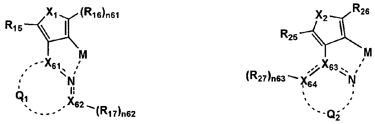
[0034] 〔式中、 X 、 X 、 X 、 X は各々炭素原子または窒素原子を表し、 Qは炭素原子、 X [In the formula, X 1, X 2, X 3 and X 3 each represent a carbon atom or a nitrogen atom, Q represents a carbon atom, X
61 62 63 64 1 61 62 63 64 1
、 X と共に 5員の芳香族複素環を形成する原子群を表し、 Qは炭素原子、 X 、 X , X represents a group of atoms that form a 5-membered aromatic heterocyclic ring, Q is a carbon atom, X, X
61 62 2 63 6461 62 2 63 64
、窒素原子と共に 5員の芳香族複素環を形成する原子群を表す。 X、 Xは 0、 S、 S Represents a group of atoms that form a 5-membered aromatic heterocycle with the nitrogen atom. X, X is 0, S, S
1 2 1 2
Oまたは SOを表す。 R は置換基を表し、 R は水素原子または置換基を表す。 R 、 Represents O or SO. R represents a substituent, and R represents a hydrogen atom or a substituent. R,
2 15 26 16 2 15 26 16
R 、R 、R はファンデルワールス体積が 20 A3以上である置換基を表す。 n61、n6R 1, R 2 and R 3 represent a substituent having a van der Waals volume of 20 A 3 or more. n61, n6
17 25 27 17 25 27
2、 n63は 0または 1を表す。但し、 n61 +n62≥lである。 Mは元素周期表における 第 8族〜第 10族の金属元素を表す。〕 2, n63 represents 0 or 1; However, n61 + n62≥l. M represents a metal element of Group 8 to Group 10 in the periodic table. ]
9.前記一般式 (2)で表される部分構造が、下記一般式 (7B)または一般式 (8B) で表される部分構造であることを特徴とする前記 3に有機エレクト口ルミネッセンス素 子材料。 9. The organic electroluminescence device according to 3 above, wherein the partial structure represented by the general formula (2) is a partial structure represented by the following general formula (7B) or the general formula (8B): material.
[0035] [化 9] 一般式 (7B) 一般式 ί8Β) [0035] [Chemical 9] General formula (7B) General formula ί8Β)

〔式中、 X 、X 、X 、X は各々炭素原子または窒素原子を表し、 Qは炭素原子、 X [Wherein, X 1, X 2, X 3, X represent a carbon atom or a nitrogen atom, Q represents a carbon atom, X
61 62 63 64 1 61 62 63 64 1
、 X と共に 6員の芳香族複素環を形成する原子群を表し、 Qは炭素原子、 X 、 X , X represents a group of atoms that form a 6-membered aromatic heterocycle with Q being a carbon atom, X, X
61 62 2 63 6461 62 2 63 64
、窒素原子と共に 6員の芳香族複素環を形成する原子群を表す。 X、 Xは 0、 S、 S Represents a group of atoms that together with the nitrogen atom form a 6-membered aromatic heterocycle. X, X is 0, S, S
1 2 1 2
Oまたは SOを表す。 R は置換基を表し、 R は水素原子または置換基を表す。 R 、
R 、 R 、 R はファンデルワールス体積が 20 A3以上である置換基を表す。 n61、 n6Represents O or SO. R represents a substituent, and R represents a hydrogen atom or a substituent. R, R 1, R 2 and R 3 each represent a substituent having a van der Waals volume of 20 A 3 or more. n61, n6
17 25 27 17 25 27
2、 n63は 0または 1を表す。但し、 n61 +n62≥lである。 Mは元素周期表における 第 8族〜第 10族の金属元素を表す。〕 2, n63 represents 0 or 1; However, n61 + n62≥l. M represents a metal element of Group 8 to Group 10 in the periodic table. ]
10.前記一般式(3)で表される部分構造が、下記一般式(9A)または一般式(10A )で表される部分構造であることを特徴とする前記 4に記載の有機エレクト口ルミネッ センス素子材料。 10. The organic electoluminescence according to 4 above, wherein the partial structure represented by the general formula (3) is a partial structure represented by the following general formula (9A) or general formula (10A): Sense element material.
[0037] [化 10] [0037] [Chemical 10]

[0038] 〔式中、 X 、 X 、 X 、 X は各々炭素原子または窒素原子を表し、 Qは炭素原子、 X [In the formula, X 1, X 2, X 3 and X 3 each represent a carbon atom or a nitrogen atom, Q represents a carbon atom, X
71 72 73 74 3 71 72 73 74 3
、 X と共に 5員の芳香族複素環を形成する原子群を表し、 Qは炭素原子、 X 、 X , X represents a group of atoms that form a 5-membered aromatic heterocyclic ring, Q is a carbon atom, X, X
71 72 4 73 7471 72 4 73 74
、窒素原子と共に 5員の芳香族複素環を形成する原子群を表す。 X、 Xは 0、 S、 S Represents a group of atoms that form a 5-membered aromatic heterocycle with the nitrogen atom. X, X is 0, S, S
3 4 3 4
Oまたは SOを表す。 R は置換基を表し、 R は水素原子または置換基を表す。 R 、 Represents O or SO. R represents a substituent, and R represents a hydrogen atom or a substituent. R,
2 35 46 36 2 35 46 36
R 、R 、R はファンデルワールス体積が 20 A3以上である置換基を表す。 n71、n7R 1, R 2 and R 3 represent a substituent having a van der Waals volume of 20 A 3 or more. n71, n7
37 45 47 37 45 47
2、 n73は 0または 1を表す。但し、 n71 +n72≥lである。 Xは 0、 S、 CH、 CHR、 C 2, n73 represents 0 or 1; However, n71 + n72≥l. X is 0, S, CH, CHR, C
0 2 0 2
(R)、 NR、 PR、 Si (R)、 C = 0、 C=NR、 SO、 SOを表す。 Rはアルキル基、シクロ (R), NR, PR, Si (R), C = 0, C = NR, SO, SO. R is an alkyl group, cyclo
2 2 2 2 2 2
アルキル基、アルケニル基、ァリール基、複素環基または芳香族複素環基を表す。 Mは元素周期表における第 8族〜第 10族の金属元素を表す。〕 Represents an alkyl group, an alkenyl group, an aryl group, a heterocyclic group or an aromatic heterocyclic group; M represents a metal element of Group 8 to Group 10 in the periodic table. ]
11.前記一般式 (4)で表される部分構造が、下記一般式 (9B)または一般式(10B )で表される部分構造であることを特徴とする前記 5に記載の有機エレクト口ルミネッ センス素子材料。 11. The organic electoluminescence according to 5 above, wherein the partial structure represented by the general formula (4) is a partial structure represented by the following general formula (9B) or the general formula (10B): Sense element material.
[0039] [化 11]
一般 [0039] [Chemical 11] General

[0040] 〔式中、 X 、 X 、 X 、 X は各々炭素原子または窒素原子を表し、 Qは炭素原子、 X [0040] [In the formula, X 1, X 2, X 3, X each represent a carbon atom or a nitrogen atom, Q represents a carbon atom, X
71 72 73 74 3 71 72 73 74 3
、 X と共に 6員の芳香族複素環を形成する原子群を表し、 Qは炭素原子、 X 、 X , X represents a group of atoms that form a 6-membered aromatic heterocycle with Q being a carbon atom, X, X
71 72 4 73 7471 72 4 73 74
、窒素原子と共に 6員の芳香族複素環を形成する原子群を表す。 X、 Xは 0、 S、 S Represents a group of atoms that together with the nitrogen atom form a 6-membered aromatic heterocycle. X, X is 0, S, S
3 4 3 4
Oまたは SOを表す。 R は置換基を表し、 R は水素原子または置換基を表す。 R 、 Represents O or SO. R represents a substituent, and R represents a hydrogen atom or a substituent. R,
2 35 46 36 2 35 46 36
R 、R 、R はファンデルワールス体積が 20 A3以上である置換基を表す。 n71、n7R 1, R 2 and R 3 represent a substituent having a van der Waals volume of 20 A 3 or more. n71, n7
37 45 47 37 45 47
2、 n73は 0または 1を表す。但し、 n71 +n72≥lである。 Xは 0、 S、 CH、 CHR、 C 2, n73 represents 0 or 1; However, n71 + n72≥l. X is 0, S, CH, CHR, C
0 2 0 2
(R)、 NR、 PR、 Si (R)、 C = 0、 C=NR、 SO、 SOを表 。 Rはアルキル基、シクロ (R), NR, PR, Si (R), C = 0, C = NR, SO, SO. R is an alkyl group, cyclo
2 2 2 2 2 2
アルキル基、アルケニル基、ァリール基、複素環基または芳香族複素環基を表す。 Represents an alkyl group, an alkenyl group, an aryl group, a heterocyclic group or an aromatic heterocyclic group;
Mは元素周期表における第 8族〜第 10族の金属元素を表す。〕 M represents a metal element of Group 8 to Group 10 in the periodic table. ]
12.前記一般式 (Z)における Mが、イリジウムまたは白金であることを特徴とする前 記 1に記載の有機エレクト口ルミネッセンス素子材料。 12. The organic electoluminescence device material as described in 1 above, wherein M in the general formula (Z) is iridium or platinum.
[0041] 13.前記 1に記載の有機エレクト口ルミネッセンス素子材料を、構成層の少なくとも 1 層に含有することを特徴とする有機エレクト口ルミネッセンス素子。 [0041] 13. An organic electoluminescence device comprising the organic electroluminescence device material described in 1 above in at least one of the constituent layers.
[0042] 14.構成層として発光層を有し、該発光層が前記 1に記載の有機エレクト口ルミネッ センス素子材料を含有することを特徴とする有機エレクト口ルミネッセンス素子。 [0042] 14. An organic electroluminescent device, comprising a luminescent layer as a constituent layer, wherein the luminescent layer contains the organic electroluminescent device material described in 1 above.
[0043] 15.前記 13に記載の有機エレクト口ルミネッセンス素子を有することを特徴とする表 示装置。 [0043] 15. A display device comprising the organic-electric-luminescence element as described in 13 above.
[0044] 16.前記 13に記載の有機エレクト口ルミネッセンス素子を有することを特徴とする照 明装置。 [0044] 16. An illuminating device comprising the organic-electric-luminescence element as described in 13 above.
発明の効果 The invention's effect
[0045] 本発明により、高い発光効率を示し、且つ発光寿命の長い有機エレクト口ルミネッセ
ンス素子材料、それを用いた有機エレクト口ルミネッセンス素子、更には該有機エレク トロルミネッセンス素子を利用した照明装置及び表示装置を提供することができた。 図面の簡単な説明 [0045] According to the present invention, an organic electoluminescence that exhibits high luminous efficiency and has a long luminous lifetime. It was possible to provide a light emitting device material, an organic electroluminescence device using the same, and an illumination device and a display device using the organic electroluminescence device. Brief Description of Drawings
[0046] [図 1]有機 EL素子力 構成される表示装置の一例を示した模式図である。 FIG. 1 is a schematic view showing an example of a display device configured with organic EL element power.
[図 2]表示部 Aの模式図である。 FIG. 2 is a schematic diagram of display unit A.
[図 3]画素を構成する駆動回路の等価回路図である。 FIG. 3 is an equivalent circuit diagram of a drive circuit constituting a pixel.
[図 4]パッシブマトリックス方式による表示装置の模式図である。 FIG. 4 is a schematic diagram of a passive matrix display device.
[図 5]照明装置の概略図である。 FIG. 5 is a schematic view of a lighting device.
[図 6]照明装置の断面図である。 FIG. 6 is a cross-sectional view of the lighting device.
符号の説明 Explanation of symbols
[0047] 1 ディスプレイ [0047] 1 display
3 画素 3 pixels
5 走査線 5 scan lines
6 データ線 6 Data line
7 電源ライン 7 Power line
10 有機 EL素子 10 Organic EL devices
11 スイッチングトランジスタ 11 Switching transistor
12 馬区動トランジスタ 12 Ma District Motion Transistor
13 コンデンサ 13 Capacitor
A 表示部 A Display section
B 制御部 B Control unit
102 ガラスカバー 102 Glass cover
105 陰極 105 cathode
106 有機 EL層 106 OLED layer
107 透明電極付きガラス基板 107 Glass substrate with transparent electrode
108 窒素ガス 108 nitrogen gas
109 捕水剤 109 Water catcher
発明を実施するための最良の形態
[0048] 本発明者等は鋭意検討を行った結果、オルトメタル錯体の配位子として金属に配 位する部分に非窒素原子を 1つ含む 5員へテロ環の 3位と 4位に結合手を持つような 部分構造を持った配位子を用いた場合に青色〜青緑色のような短波長の発光を持 ち、高い発光効率を示すと共に発光寿命が大幅に改善されることを見出した。なお、 本発明にお 、ては記載されて 、る部分構造は、その互変異性体の部分構造も含む BEST MODE FOR CARRYING OUT THE INVENTION [0048] As a result of intensive studies, the inventors of the present invention have bonded to the 3rd and 4th positions of a 5-membered heterocycle containing one non-nitrogen atom in the portion coordinated to the metal as the ligand of the ortho metal complex. It has been found that when a ligand with a hand-held partial structure is used, it emits light with a short wavelength such as blue to blue-green, showing high luminous efficiency and greatly improving the luminous lifetime. It was. Note that the partial structure described in the present invention includes a partial structure of a tautomer thereof.
[0049] 以下、本発明に係る各構成要素の詳細について、順次説明する。 [0049] Details of each component according to the present invention will be sequentially described below.
[0050] 本発明の有機エレクト口ルミネッセンス素子材料にぉ 、ては、前記一般式 (Z)で表 される部分構造を有するオルトメタル錯体を含有することを特徴とする。 [0050] The organic electoluminescence device material of the present invention is characterized by containing an ortho metal complex having a partial structure represented by the general formula (Z).
[0051] 請求の範囲第 1項に記載の前記一般式 (Z)において、 Xは 0、 S、 SOまたは SOを [0051] In the general formula (Z) according to claim 1, X is 0, S, SO or SO.
2 表し、 Xは 2価の基または単結合を表す。 Rは置換基を表す。 Rは水素原子または 2 represents, X represents a divalent group or a single bond. R represents a substituent. R is a hydrogen atom or
1 a b 1 a b
置換基を表す。 Lは窒素原子と共に 5〜7員の芳香族複素環を形成する。 Mは元素 周期表における第 8族〜第 10族の金属元素を表す。 Mとしては、イリジウムまたは白 金であることが好ましい。 Represents a substituent. L forms a 5- to 7-membered aromatic heterocycle with the nitrogen atom. M represents a group 8-10 metal element in the periodic table. M is preferably iridium or gold.
[0052] 更に、本発明の有機エレクト口ルミネッセンス素子材料においては、前記一般式 (Z[0052] Further, in the organic electoluminescence device material of the present invention, the general formula (Z
)で表される部分構造が、前記一般式 (1)〜(4)から選ばれる少なくとも 1種の部分構 造であることが好ましい。 ) Is preferably at least one partial structure selected from the general formulas (1) to (4).
[0053] 本発明に係る前記一般式( 1)〜 (4)からなる部分構造群から選択される少なくとも 1 種のオルトメタル錯体の有機エレクト口ルミネッセンス素子材料における含有層として は、発光層または正孔阻止層が好ましぐまた発光層に含有する場合は発光層中の 発光ドーパントとして用いることにより、本発明の目的である有機 EL素子の発光寿命 の長寿命化を達成することができる。 [0053] The inclusion layer in the organic electoluminescence device material of at least one orthometal complex selected from the partial structure group consisting of the general formulas (1) to (4) according to the present invention includes a light emitting layer or a positive layer. When the hole blocking layer is preferred and contained in the light-emitting layer, it can be used as a light-emitting dopant in the light-emitting layer, thereby achieving an increase in the light-emitting lifetime of the organic EL device that is the object of the present invention.
[0054] 以下、本発明に係る一般式( 1)〜 (4)で表される部分構造を有するオルトメタル錯 体の詳細について説明する。 [0054] Details of the orthometal complex having the partial structure represented by the general formulas (1) to (4) according to the present invention will be described below.
[0055] 《一般式(1)で表される部分構造を有するオルトメタル錯体》 [0055] << Orthometal Complex Having Partial Structure Represented by General Formula (1) >>
請求の範囲第 2項に記載の前記一般式(1)において、 X は 0、 S、 SOまたは SO In the general formula (1) according to claim 2, X is 0, S, SO or SO
10 2 を表し、 Rは置換基を表す。 Rは水素原子または置換基を表す。 X 、 X 、 X 、 X 10 2 represents, and R represents a substituent. R represents a hydrogen atom or a substituent. X, X, X, X
1 2 11 12 13 14 は各々 C、C—R 、N、N—R 、 Oまたは Sを表し、且つ窒素原子と共に 5員の芳香
族複素環を形成する。 R は水素原子または置換基を表す。 Mは元素周期表におけ 1 2 11 12 13 14 each represents C, C—R, N, N—R, O or S, and a 5-membered fragrance together with a nitrogen atom Forming a family heterocycle. R represents a hydrogen atom or a substituent. M in the periodic table
11 11
る第 8族〜第 10族の金属元素を表す。 Group 8 to Group 10 metal elements.
[0056] R、R が表す置換基としては、例えば、アルキル基 (例えば、メチル基、ェチル基、 [0056] Examples of the substituent represented by R and R include an alkyl group (for example, a methyl group, an ethyl group,
1 11 1 11
イソプロピル基、ヒドロキシェチル基、メトキシメチル基、トリフルォロメチル基、 tーブチ ル基、ペンチル基、ォクチル基、ノ-ル基、デシル基等)、シクロアルキル基 (例えば、 シクロペンチル基、シクロへキシル基等)、ァラルキル基(例えば、ベンジル基、 2—フ エネチル基等)、ァリール基(例えば、フエ-ル基、 p—クロ口フエニル基、メシチル基、 トリル基、キシリル基、ビフヱ-リル基、ナフチル基、アントリル基、フエナントリル基等) 、複素環基 (例えば、ピロリジル基、イミダゾリル基、モルホリル基、ォキサゾリジル基 等)、芳香族複素環基 (例えば、フリル基、チェニル基、ピリジル基、ピリダジニル基、 ピリミジニル基、ビラジニル基、トリアジニル基、イミダゾリル基、ピラゾリル基、チアゾリ ル基、キナゾリニル基、カルバゾリル基、カルボリ-ル基、ジァザカルバゾリル基 (ジァ ザカルバゾリル基とは、該カルボリニル基のカルボリン環を構成する炭素原子の任意 にひとつが窒素原子で置換されたものを示す。)、フタラジュル基等)、アルコキシ基( 例えば、エトキシ基、イソプロポキシ基、ブトキシ基等)、ァリールォキシ基 (例えば、フ エノキシ基、ナフチルォキシ基等)、シァノ基、水酸基、アルケニル基 (例えば、ビュル 基等)、スチリル基、ハロゲン原子 (例えば、塩素原子、臭素原子、沃素原子、フッ素 原子等)等が挙げられ、より好ましくはアルキル基、シクロアルキル基、ァリール基、複 素環基、芳香族複素環基である。これらの基は更に置換されていてもよい。 Isopropyl group, hydroxyethyl group, methoxymethyl group, trifluoromethyl group, tert-butyl group, pentyl group, octyl group, nor group, decyl group, etc.), cycloalkyl group (for example, cyclopentyl group, cyclohexyl group) Xyl group, etc.), aralkyl groups (eg, benzyl group, 2-phenethyl group, etc.), aryl groups (eg, phenyl group, p-chlorophenyl group, mesityl group, tolyl group, xylyl group, biphenyl-yl). Group, naphthyl group, anthryl group, phenanthryl group, etc.), heterocyclic group (eg, pyrrolidyl group, imidazolyl group, morpholyl group, oxazolidyl group, etc.), aromatic heterocyclic group (eg, furyl group, chenyl group, pyridyl group, Pyridazinyl group, pyrimidinyl group, birazinyl group, triazinyl group, imidazolyl group, pyrazolyl group, thiazolyl group, quinazolyl Group, carbazolyl group, carbolyl group, diazacarbazolyl group (Diazacarbazolyl group is a group in which any one of the carbon atoms constituting the carboline ring of the carbolinyl group is substituted with a nitrogen atom. ), Phthaladyl group, etc.), alkoxy group (eg, ethoxy group, isopropoxy group, butoxy group, etc.), aryloxy group (eg, phenoxy group, naphthyloxy group, etc.), cyano group, hydroxyl group, alkenyl group (eg, A butyl group, a styryl group, a halogen atom (eg, a chlorine atom, a bromine atom, an iodine atom, a fluorine atom, etc.), more preferably an alkyl group, a cycloalkyl group, an aryl group, a heterocyclic group, an aromatic group. Group heterocyclic group. These groups may be further substituted.
[0057] X 、X 、X 、X は各々 C、C— R 、 N、 N— R 、 Oまたは Sを表し、且つ窒素原子 [0057] X 1, X 2, X 3 and X 4 each represent C, C—R, N, N—R, O or S, and a nitrogen atom
11 12 13 14 11 11 11 12 13 14 11 11
と共に 5員の芳香族複素環を形成するが、カゝかる 5員の芳香族複素環として具体的 には、イミダゾール環、ピラゾール環、イソチアゾール環、イソキサゾール環、ォキサゾ ール環、チアゾール環、トリァゾール環等が挙げられる。 Together with a 5-membered aromatic heterocycle, specific examples of the 5-membered aromatic heterocycle include imidazole ring, pyrazole ring, isothiazole ring, isoxazole ring, oxazole ring, thiazole ring, And a triazole ring.
[0058] 本発明においては、本発明に係る前記一般式(1)で表される部分構造が、下記一 般式(1)—1〜(1)—15で表される部分構造群力も選択される少なくとも一つの部分 構造であることが好ましい。 [0058] In the present invention, the partial structure represented by the general formula (1) according to the present invention is also selected from the partial structure group forces represented by the following general formulas (1) -1 to (1) -15 It is preferable that at least one partial structure is formed.
[0059] [化 12]
[0059] [Chemical 12]


[0060] 上記一般式(1) 1〜(: 0—15において、 R 、R は各々置換基を表し、 R は水 [0060] In the above general formulas (1) 1 to (: 0-15, R 1 and R 2 each represent a substituent, and R 1 represents water
12 14 13 素原子または置換基を表す。 nlは各々 0〜2から選ばれる整数を表す。 X は 0、 S、 12 14 13 Elemental atom or substituent. nl represents an integer selected from 0 to 2, respectively. X is 0, S,
15 15
SOまたは SOを表し、 X は各々〉 N— R 、— O または— S を表す。 R はアル SO represents SO or SO, and X represents> N—R, —O or —S, respectively. R is al
2 16 15 15 キル基、シクロアルキル基、ァルケ-ル基、ァリール基、複素環基または芳香族複素 環基を表す。 Mは元素周期表における第 8族〜第 10族の金属元素を表す。 2 16 15 15 Represents a kill group, cycloalkyl group, alkyl group, aryl group, heterocyclic group or aromatic heterocyclic group. M represents a metal element of Group 8 to Group 10 in the periodic table.
[0061] R 、 R 、 R が表す置換基としては、前記一般式(1)の R、 R が表す置換基と同 [0061] The substituents represented by R 1, R 2, and R 3 are the same as the substituents represented by R 1 and R 2 in the general formula (1).
12 14 13 1 11 12 14 13 1 11
様のものが挙げられる。 R の具体的基は、後述する一般式(3)の Rと同様のものが Something like that. The specific group of R is the same as R in the general formula (3) described later.
15 15
挙げられる。 Can be mentioned.
[0062] 更に、本発明においては、本発明に係る前記一般式(1)で表される部分構造が、
前記一般式(7A)または一般式 (8A)で表される部分構造であることが好ま 、。 [0062] Further, in the present invention, the partial structure represented by the general formula (1) according to the present invention is: It is preferably a partial structure represented by the general formula (7A) or the general formula (8A).
[0063] 前記一般式(7A)または一般式 (8A)において、 X 、X 、X 、X は各々炭素原紙 [0063] In the general formula (7A) or the general formula (8A), X 1, X 2, X 3 and X 4 are each a carbon base paper.
61 62 63 64 61 62 63 64
または窒素原子を表し、 Qは炭素原子、 X 、 X と共に 5員の芳香族複素環を形成 Or represents a nitrogen atom, Q forms a 5-membered aromatic heterocycle with carbon atom, X and X
1 61 62 1 61 62
する原子群を表し、 Qは炭素原子、 X 、 X 、窒素原子と共に 5員の芳香族複素環を Q represents a 5-membered aromatic heterocycle with carbon, X, X and nitrogen atoms.
2 63 64 2 63 64
形成する原子群を表す。 X、 Xは 0、 S、 SOまたは SOを表す。 R は置換基を表し Represents the atomic group to be formed. X and X represent 0, S, SO or SO. R represents a substituent
1 2 2 15 1 2 2 15
、R は水素原子または置換基を表す。 R 、R 、R 、R はファンデルワールス体積 , R represents a hydrogen atom or a substituent. R, R, R, R are van der Waals volumes
26 16 17 25 27 26 16 17 25 27
力 S20A3以上である置換基を表す。 n61、 n62、 n63は 0または 1を表す。但し、 n61 +n62≥ 1である。 Mは元素周期表における第 8族〜第 10族の金属元素を表す。 Force S20A represents a substituent that is 3 or more. n61, n62, and n63 represent 0 or 1. However, n61 + n62≥1. M represents a metal element of Group 8 to Group 10 in the periodic table.
[0064] R 、R が表す置換基としては、前記一般式(1)の R、R が表す置換基と同様のも [0064] The substituents represented by R 1 and R 2 are the same as the substituents represented by R 1 and R 2 in the general formula (1).
15 26 1 11 15 26 1 11
のが挙げられる。 Qは炭素原子、 X 、 X と共に 5員の芳香族複素環を形成する原 Can be mentioned. Q is an element that forms a 5-membered aromatic heterocycle with carbon atoms, X and X.
1 61 62 1 61 62
子群を表すが、ここで 5員の芳香族複素環としてはォキサゾール環、チオフ ン環、 フラン環、ピロール環、イミダゾール環、ピラゾール環、トリァゾール環等が挙げられる 。また Qは炭素原子、 X 、 X 、窒素原子と共に 5員の芳香族複素環を形成する原 The 5-membered aromatic heterocycle includes an oxazole ring, a thiophene ring, a furan ring, a pyrrole ring, an imidazole ring, a pyrazole ring, and a triazole ring. Q is an element that forms a 5-membered aromatic heterocycle with carbon, X, X, and nitrogen.
2 63 64 2 63 64
子群を表すが、 5員の芳香族複素環としては、ォキサゾール環、ピロール環、イミダゾ ール環、ピラゾール環、トリァゾール環等が挙げられる。 The 5-membered aromatic heterocycle includes an oxazole ring, pyrrole ring, imidazole ring, pyrazole ring, triazole ring and the like.
[0065] R 、R 、R 、R はファンデルワールス体積が 20 A3以上である置換基を表すが、 [0065] R 1, R 2, R 3 and R 4 each represent a substituent having a van der Waals volume of 20 A 3 or more,
16 17 25 27 16 17 25 27
置換基のファンデルワールス (VDW)体積とは、アクセルリス社製分子シミュレーショ ンソフト Cerius 2を用 、て求められるパラメーターを用いるが、ベンゼン環に置換基を 導入し、 Dreiding Force Fieldを用いて、 MM計算で分子構造を最適化して、 Co nnoly Surfaceを用いて求めた Volume値と定義する。具体的な置換基のファンデ ルヮーノレス (VDW)体積を下記に示す。 The van der Waals (VDW) volume of the substituent is a parameter obtained using the molecular simulation software Cerius 2 manufactured by Accelrys, Inc., but the substituent is introduced into the benzene ring and the Dreiding Force Field is used. Optimized molecular structure by MM calculation and defined as Volume value obtained by using Connnoly Surface. The specific volume of van derunoles (VDW) of the substituent is shown below.
[0066] 置換基 A3 [0066] Substituent A 3
メチノレ基 25. 4 Methinore group 25.4
ェチル基 42. 6 Ethyl group 42.6
イソプロピノレ基 59. 5 Isopropinole group 59.5
tert—ブチノレ基 76. 2 tert-Butinole group 76. 2
フエ-ル基 74. 9 Phenol group 74.9
メトキシ基 34. 0
アミノ基 22. 2 Methoxy group 34.0 Amino group 22.2
ヒドロキシル基 16. 7 Hydroxyl group 16.7
塩素原子 22. 4 Chlorine atom 22.4
臭素原子 26. 5 Bromine atom 26.5
フッ素原子 13. 3 Fluorine atom 13.3
トリフルォロメチル基 42. 5 Trifluoromethyl group 42.5
従って R 、R 、R 、R としては、具体的にはメチル基、ェチル基、イソプロピル基 Accordingly, R 1, R 2, R 3, and R 4 are specifically methyl, ethyl, and isopropyl groups.
16 17 25 27 16 17 25 27
、 tert—ブチル基、フエニル基、メトキシ基、アミノ基、塩素原子、臭素原子、トリフル ォロメチル基等が挙げられる。 Tert-butyl group, phenyl group, methoxy group, amino group, chlorine atom, bromine atom, trifluoromethyl group and the like.
[0067] 《一般式 (2)で表される部分構造を有するオルトメタル錯体》 [0067] << Orthometal Complex Having Partial Structure Represented by General Formula (2) >>
請求の範囲第 3項に記載の前記一般式(2)において、 X は 0、 S、 SOまたは SO In the general formula (2) according to claim 3, X is 0, S, SO or SO
20 2 を表し、 R 20 represents 2 and R
3は置換基を表す。 R 3 represents a substituent. R
4は水素原子または置換基を表す。 X 、 X 、 X 、 X 4 represents a hydrogen atom or a substituent. X, X, X, X
21 22 23 24 は各々 C R または Nを表し、且つ炭素原子、窒素原子と共に 6員の芳香族複素環 21 22 23 24 each represents C R or N, and together with a carbon atom and a nitrogen atom, a 6-membered aromatic heterocycle
21 twenty one
を形成する。 R Form. R
21は水素原子または置換基を表す。 Mは元素周期表における第 8族 21 represents a hydrogen atom or a substituent. M is group 8 in the periodic table
〜第 10族の金属元素を表す。 ~ Represents Group 10 metal elements.
[0068] R、 R、 R が表す置換基としては、前記一般式(1)の R、 R が表す置換基と同様 [0068] The substituents represented by R, R and R are the same as the substituents represented by R and R in the general formula (1).
3 4 21 1 11 3 4 21 1 11
のものが挙げられる。 X 、X 、X 、X は各々 C—R または Nを表し、且つ炭素原子 Can be mentioned. X 1, X 2, X 3 and X each represent C—R or N, and a carbon atom
21 22 23 24 21 21 22 23 24 21
、窒素原子と共に 6員の芳香族複素環を形成するが、力かる 6員の芳香族複素環とし て具体的には、ピリジン環、ピリミジン環、ピリダジン環、ピラジン環等が挙げられる。 A 6-membered aromatic heterocycle is formed together with the nitrogen atom, and specific examples of the powerful 6-membered aromatic heterocycle include a pyridine ring, a pyrimidine ring, a pyridazine ring, and a pyrazine ring.
[0069] 本発明においては、本発明に係る前記一般式 (2)で表される部分構造が、下記一 般式 (2)— 1〜(2)— 6で表される部分構造群力も選択される少なくとも一つの部分 構造であることが好ましい。 [0069] In the present invention, the partial structure represented by the general formula (2) according to the present invention is also selected from the partial structural group forces represented by the following general formulas (2) -1 to (2) -6 It is preferable that at least one partial structure is formed.
[0070] [化 13]
 [0070] [Chemical 13]
[0071] 上記一般式(2)— 1〜(2)—6において、 R 、R は各々置換基を表し、 R は水素 [0071] In the general formulas (2) -1 to (2) -6, R 1 and R 2 each represent a substituent, and R 1 represents hydrogen
22 24 23 原子または置換基を表す。 n2は 0〜2から選ばれる整数を表す。 X は 0、 S、 SOま 22 24 23 represents an atom or a substituent. n2 represents an integer selected from 0 to 2. X is 0, S, SO
25 twenty five
たは SOを表す。 Mは元素周期表における第 8族〜第 10族の金属元素を表す。 Or SO. M represents a metal element of Group 8 to Group 10 in the periodic table.
2 2
[0072] R 、 R 、 R が表す置換基としては、前記一般式(1)の R、 R が表す置換基と同 [0072] The substituents represented by R 1, R 2 and R 3 are the same as the substituents represented by R and R in the general formula (1).
22 24 23 1 11 22 24 23 1 11
様のものが挙げられる。 Something like that.
[0073] また、前記一般式 (2)で表される部分構造が、前記一般式 (5)で表される部分構造 であることが好ましい。 [0073] The partial structure represented by the general formula (2) is preferably a partial structure represented by the general formula (5).
[0074] 請求の範囲第 6項に記載の前記一般式(5)において、 R は置換基を表し、 R は [0074] In the general formula (5) according to claim 6, R represents a substituent, and R represents
51 52 各々水素原子または置換基を表す。 R 51 52 Each represents a hydrogen atom or a substituent. R
51と R 51 and R
52の少なくとも一方は電子供与性の置換 基または電子吸引性の置換基である。 X は 0、 S、 SOまたは SOを表す。 R は置換 At least one of 52 is an electron donating substituent or an electron withdrawing substituent. X represents 0, S, SO or SO. R is a substitution
51 2 50 基を表し、 n51は 0〜3から選ばれる整数を表す。 Xaは—N (Ra)、—O—Raまたは 51 2 50 represents a group, and n51 represents an integer selected from 0 to 3. Xa is —N (Ra), —O—Ra or
2 2
S— Raを表す。 Raはアルキル基、シクロアルキル基、ァルケ-ル基、ァリール基、 複素環基または芳香族複素環基を表す。 Xaが— N (Ra) の場合、 2つの Raは同じで S—Ra Ra represents an alkyl group, a cycloalkyl group, an alkyl group, an aryl group, a heterocyclic group or an aromatic heterocyclic group. If Xa is — N (Ra), the two Ras are the same
2 2
あっても異なって 、てもよ 、。 Mは元素周期表における第 8族〜第 10族の金属元素 を表す。 It ’s different, but it ’s different. M represents a metal element of Group 8 to Group 10 in the periodic table.
[0075] R 、 R 、 R が表す置換基としては、前記一般式(1)の R、 R が表す置換基と同 [0075] The substituents represented by R 1, R 2 and R 3 are the same as the substituents represented by R and R in the general formula (1).
51 52 50 1 11 51 52 50 1 11
様のものが挙げられる。 Raの具体的基は後述する一般式(3)の Rと同様のものが挙 げられる。 R と R の少なくとも一方は電子供与性の置換基または電子吸引性の置 Something like that. Specific examples of Ra include the same groups as R in formula (3) described later. At least one of R and R is an electron-donating substituent or an electron-withdrawing moiety.
51 52 51 52
換基である力 ここで電子供与性の置換基はハメットの置換基定数 σ ρが負の値を示
す基のことであり、具体的にはヒドロキシ基、アルコキシ基 (例えば、メトキシ基)、ァシ ルォキシ基 (例えば、ァセチルォキシ基、ベンゾィルォキシ基)、アミノ基、ジメチルァ ミノ基、ァセチルァミノ基、アルキル基 (例えば、メチル基、プロピル基)、ァリール基( 例えば、フエニル基、メシチル基)等が挙げられる。一方、電子吸引性の置換基はハ メットの置換基定数 σ ρが正の値を示す基のことであり、具体的にはシァノ基、アルコ キシカルボ-ル基、ァリールォキシカルボ-ル基、力ルバモイル基、イミノ基、 Ν原子 で置換したイミノ基、チォカルボ-ル基、スルファモイル基、アルキルスルホ-ル基、 ァリールスルホ-ル基、ニトロ基、ハロゲン原子、パーフルォロアルキル基、パーフル ォロアルカンアミド基、スルホンアミド基、ァシル基、ホルミル基、ホスホリル基、カルボ キシ基 (またはその塩)、スルホ基 (またはその塩)、ヘテロ環基、アルケニル基、アル キニル基、ァシルォキシ基、ァシルチオ基、スルホ-ルォキシ基、またはこれら電子 吸引性基で置換されたァリール基等である。ここにへテロ環基としては、飽和もしくは 不飽和のヘテロ環基で、例えばピリジル基、キノリル基、キノキサリニル基、ピラジ二 ル基、ベンゾトリァゾリル基、イミダゾリル基、ベンツイミダゾリル基、ヒダントインー 1 ィル基、スクシンイミド基、フタルイミド基等がその例として挙げられる。 Here, the electron-donating substituent has a negative value for Hammett's substituent constant σ ρ. Specifically, hydroxy group, alkoxy group (for example, methoxy group), acyloxy group (for example, acetyloxy group, benzoyloxy group), amino group, dimethylamino group, acetylamino group, alkyl group ( For example, a methyl group, a propyl group), an aryl group (for example, a phenyl group, a mesityl group), etc. are mentioned. On the other hand, an electron-withdrawing substituent is a group in which Hammett's substituent constant σ ρ exhibits a positive value, and specifically, a cyano group, an alkoxycarbonyl group, an aryloxycarbol group. , Force rubermoyl group, imino group, imino group substituted with Ν atom, thiocarbole group, sulfamoyl group, alkylsulfol group, arylsulfol group, nitro group, halogen atom, perfluoroalkyl group, perfluoro Loalcanamide group, sulfonamide group, acyl group, formyl group, phosphoryl group, carboxyl group (or salt thereof), sulfo group (or salt thereof), heterocyclic group, alkenyl group, alkynyl group, acyloxy group, acylylthio Group, a sulfo-loxy group, or an aryl group substituted with these electron-withdrawing groups. Here, the heterocyclic group is a saturated or unsaturated heterocyclic group, for example, pyridyl group, quinolyl group, quinoxalinyl group, pyrazinyl group, benzotriazolyl group, imidazolyl group, benzimidazolyl group, hydantoin 1 Examples thereof include a ruthenium group, a succinimide group, and a phthalimide group.
[0076] また、前記一般式(2)で表される部分構造力 前記一般式(7Β)または一般式 (8Β )で表される部分構造であることが好ま 、。 [0076] The partial structural force represented by the general formula (2) is preferably a partial structure represented by the general formula (7 () or the general formula (8Β).
[0077] 前記一般式(7Β)または一般式 (8Β)において、 X 、Χ 、Χ 、Χ は各々炭素原子 [0077] In the general formula (7Β) or the general formula (8Β), X, Χ, Χ, and Χ are each a carbon atom.
61 62 63 64 61 62 63 64
または窒素原子を表し、 Qは炭素原子、 X 、 X と共に 6員の芳香族複素環を形成 Or represents a nitrogen atom, Q forms a 6-membered aromatic heterocycle with carbon atom, X and X
1 61 62 1 61 62
する原子群を表し、 Qは炭素原子、 X 、 X 、窒素原子と共に 6員の芳香族複素環を Q represents a 6-membered aromatic heterocycle with carbon, X, X and nitrogen atoms.
2 63 64 2 63 64
形成する原子群を表す。 X、 Xは 0、 S、 SOまたは SOを表す。 R は置換基を表し、 Represents the atomic group to be formed. X and X represent 0, S, SO or SO. R represents a substituent,
1 2 2 15 1 2 2 15
R は水素原子または置換基を表す。 R 、R 、R 、R はファンデルワールス体積が R represents a hydrogen atom or a substituent. R, R, R, R are van der Waals volumes
26 16 17 25 27 26 16 17 25 27
20 A3以上である置換基を表す。 n61、 n62、 1163【ま0また【ま1を表す。但し、 n61 +n 62≥1である。 Mは元素周期表における第 8族〜第 10族の金属元素を表す。 20 A represents a substituent that is 3 or more. n61, n62, 1163 [0 or 1]. However, n61 + n 62≥1. M represents a metal element of Group 8 to Group 10 in the periodic table.
[0078] R 、R が表す置換基としては、前記一般式(1)の R、R が表す置換基と同様のも [0078] The substituents represented by R 1 and R 2 are the same as the substituents represented by R 1 and R 2 in the general formula (1).
15 26 1 11 15 26 1 11
のが挙げられる。 Qは炭素原子、 X 、 X と共に 6員の芳香族複素環を形成する原 Can be mentioned. Q is an element that forms a 6-membered aromatic heterocycle with carbon atoms, X and X.
1 61 62 1 61 62
子群を表すが、ここで 6員の芳香族複素環としては、ピリジン環、ピリダジン環、ピリミ ジン環、ピラジン環、トリアジン環等が挙げられる。また Qは炭素原子、 X 、 X 、窒素
原子と共に 5員の芳香族複素環を形成する原子群を表すが、 6員の芳香族複素環と しては、ピリジン環、ピリダジン環、ピリミジン環、ピラジン環、トリアジン環等が挙げら れる。 The six-membered aromatic heterocycle includes a pyridine ring, a pyridazine ring, a pyrimidine ring, a pyrazine ring, and a triazine ring. Q is a carbon atom, X, X, nitrogen This represents an atomic group that forms a 5-membered aromatic heterocycle with an atom. Examples of the 6-membered aromatic heterocycle include a pyridine ring, a pyridazine ring, a pyrimidine ring, a pyrazine ring, and a triazine ring.
[0079] R 、R 、R 、R はファンデルワールス体積が 20 A3以上である置換基を表し、前 [0079] R 1, R 2, R 3 and R 4 represent a substituent having a van der Waals volume of 20 A 3 or more,
16 17 25 27 16 17 25 27
記一般式 (7A)または一般式 (8A)と同様の基を挙げることができる。 Examples thereof include the same groups as those represented by the general formula (7A) or the general formula (8A).
[0080] 《一般式 (3)で表される部分構造を有するオルトメタル錯体》 [0080] << Orthometal Complex Having Partial Structure Represented by General Formula (3) >>
請求の範囲第 4項に記載の前記一般式(3)において、 X は 0、 S、 SOまたは SO In the general formula (3) according to claim 4, X is 0, S, SO or SO
30 2 を表し、 Rは置換基を表す。 Rは水素原子または置換基を表す。 X 、 X 、 X 、 X 30 2 and R represents a substituent. R represents a hydrogen atom or a substituent. X, X, X, X
5 6 31 32 33 34 は各々 C、C—R 、N、N—R 、 Oまたは Sを表し、且つ窒素原子と共に 5員の芳香 5 6 31 32 33 34 each represents C, C—R, N, N—R, O or S, and a 5-membered fragrance together with a nitrogen atom
31 31 31 31
族複素環を形成する。 R は水素原子または置換基を表す。 Xは 0、 S、 CH、 CHR Forming a family heterocycle. R represents a hydrogen atom or a substituent. X is 0, S, CH, CHR
31 0 2 31 0 2
、 C (R) 、 NR、 PR、 Si (R)、 C = 0、 C=NR、 SO、 SOを表す。 Rはアルキル基、シ, C (R), NR, PR, Si (R), C = 0, C = NR, SO, SO. R is an alkyl group,
2 2 2 2 2 2
クロアルキル基、アルケニル基、ァリール基、複素環基または芳香族複素環基を表す 。 Mは元素周期表における第 8族〜第 10族の金属元素を表す。 A chloroalkyl group, an alkenyl group, an aryl group, a heterocyclic group or an aromatic heterocyclic group; M represents a metal element of Group 8 to Group 10 in the periodic table.
[0081] R、 R、 R が表す置換基としては、前記一般式(1)の R、 R が表す置換基と同様 [0081] The substituents represented by R, R and R are the same as the substituents represented by R and R in the general formula (1).
5 6 31 1 11 5 6 31 1 11
のものが挙げられる。 X 、X 、X 、X は各々 C、C— R 、N、N— R 、 Oまたは Sを Can be mentioned. X 1, X 2, X 3, and X 3 are C, C—R, N, N—R, O, or S, respectively.
31 32 33 34 31 11 31 32 33 34 31 11
表し、且つ窒素原子と共に 5員の芳香族複素環を形成するが、かかる 5員の芳香族 複素環として具体的には、前記一般式(1)で挙げられたものである。 And a 5-membered aromatic heterocycle together with the nitrogen atom. Specific examples of the 5-membered aromatic heterocycle include those listed in the general formula (1).
[0082] Rは、アルキル基(例えば、メチル基、ェチル基、イソプロピル基、ヒドロキシェチル 基、メトキシメチル基、トリフルォロメチル基、 t ブチル基、ペンチル基、ォクチル基、 ノ-ル基、デシル基等)、シクロアルキル基(例えば、シクロペンチル基、シクロへキシ ル基等)、アルケニル基 (例えば、ビニル基等)、ァリール基 (例えば、フ ニル基、 p ークロロフヱ-ル基、メシチル基、トリル基、キシリル基、ビフヱ-リル基、ナフチル基、 アントリル基、フ ナントリル基等)、複素環基 (例えば、ピロリジル基、イミダゾリル基、 モルホリル基、ォキサゾリジル基等)、芳香族複素環基 (例えば、フリル基、チェ-ル 基、ピリジル基、ピリダジニル基、ピリミジニル基、ピラジュル基、トリアジニル基、イミダ ゾリル基、ピラゾリル基、チアゾリル基、キナゾリニル基、カルバゾリル基、カルボリニル 基、ジァザカルバゾリル基 (ジァザカルバゾリル基とは、該カルボリ-ル基のカルボリ ン環を構成する炭素原子の任意にひとつが窒素原子で置換されたものを示す。)、フ
タラジニル基等)を表す。 [0082] R represents an alkyl group (for example, a methyl group, an ethyl group, an isopropyl group, a hydroxyethyl group, a methoxymethyl group, a trifluoromethyl group, a tbutyl group, a pentyl group, an octyl group, a nor group, Decyl group, etc.), cycloalkyl group (eg, cyclopentyl group, cyclohexyl group, etc.), alkenyl group (eg, vinyl group, etc.), aryl group (eg, phenyl group, p-chlorophenyl group, mesityl group, A tolyl group, a xylyl group, a biphfylyl group, a naphthyl group, an anthryl group, a phenanthryl group, etc.), a heterocyclic group (eg, pyrrolidyl group, imidazolyl group, morpholyl group, oxazolidyl group, etc.), an aromatic heterocyclic group (eg, , Furyl group, chael group, pyridyl group, pyridazinyl group, pyrimidinyl group, pyrajur group, triazinyl group, imidazolyl group, pyrazolyl group Thiazolyl group, quinazolinyl group, carbazolyl group, carbolinyl group, diazacarbazolyl group (Diazacarbazolyl group is any one of the carbon atoms constituting the carbocyclic ring of the carboryl group. Indicates an atom-substituted one), Represents a tarazinyl group and the like.
[0083] また、前記一般式 (3)で表される部分構造が、下記一般式 (3)— 1〜(3)— 15で表 される部分構造群力も選択される少なくとも一つの部分構造であることが好ましい。 [0083] Further, the partial structure represented by the general formula (3) is at least one partial structure in which partial structural group forces represented by the following general formulas (3) -1 to (3) -15 are also selected. Preferably there is.
[0084] [化 14] [0084] [Chemical 14]

[0085] 上記ー般式(3)—1〜(3)—15にぉぃて、1 、R は各々置換基を表し、 R は水 [0085] In the above general formulas (3) -1 to (3) -15, 1 and R each represent a substituent, and R represents water.
32 34 33 素原子または置換基を表す。 n3は各々 0〜2から選ばれる整数を表す。 X は 0、 S、 32 34 33 Represents an elementary atom or a substituent. n3 represents an integer selected from 0 to 2, respectively. X is 0, S,
35 35
SOまたは SOを表し、 X は各々〉 N— R 、— O—または— S—を表す。 R はアル SO represents SO or SO, and X represents> N—R, —O— or —S—, respectively. R is al
2 36 35 35 キル基、シクロアルキル基、ァルケ-ル基、ァリール基、複素環基または芳香族複素 環基を表す。 Xは 0、 S、 CH、 CHR、 C (R)、 NR、 PR、 Si (R)、 C = 0、 C=NR、 2 36 35 35 Represents a kill group, cycloalkyl group, alkyl group, aryl group, heterocyclic group or aromatic heterocyclic group. X is 0, S, CH, CHR, C (R), NR, PR, Si (R), C = 0, C = NR,
SO、 SOを表す。 Rはアルキル基、シクロアルキル基、ァルケ-ル基、ァリール基、複
素環基または芳香族複素環基を表す。 Mは元素周期表における第 8族〜第 10族の 金属元素を表す。 Represents SO and SO. R represents an alkyl group, a cycloalkyl group, an alkyl group, an aryl group, a double group Represents a unicyclic group or an aromatic heterocyclic group. M represents a metal element of Group 8 to Group 10 in the periodic table.
[0086] R 、 R 、 R が表す置換基としては、前記一般式(1)の R、 R が表す置換基と同 [0086] The substituents represented by R 1, R 2 and R 3 are the same as the substituents represented by R and R in the general formula (1).
32 34 33 1 11 32 34 33 1 11
様のものが挙げられる。 R 、 Rの具体的基は前記一般式(3)の Rと同様のものが挙 Something like that. Specific groups of R 1 and R 2 are the same as those of R in the general formula (3).
35 35
げられる。 I can get lost.
[0087] また、前記一般式(3)で表される部分構造力 前記一般式(9A)または一般式(10 Further, the partial structural force represented by the general formula (3) The general formula (9A) or the general formula (10
A)で表される部分構造であることが好ま 、。 The partial structure represented by A) is preferred.
[0088] 前記一般式(9A)または一般式(10A)において、 X 、X 、X 、X は各々炭素原 [0088] In the general formula (9A) or the general formula (10A), X 1, X 2, X 3, and X 4 are each a carbon atom.
71 72 73 74 71 72 73 74
子または窒素原子を表し、 Qは炭素原子、 X 、 X と共に 5員の芳香族複素環を形 Represents a child atom or a nitrogen atom, and Q forms a 5-membered aromatic heterocycle with carbon atom, X and X
3 71 72 3 71 72
成する原子群を表し、 Qは炭素原子、 X 、 X 、窒素原子と共に 5員の芳香族複素 Q represents a 5-membered aromatic complex with carbon, X, X and nitrogen atoms.
4 73 74 4 73 74
環を形成する原子群を表す。 X、 Xは 0、 S、 SOまたは SOを表す。 R は置換基を A group of atoms forming a ring is represented. X and X represent 0, S, SO or SO. R is a substituent
3 4 2 35 3 4 2 35
表し、 R は水素原子または置換基を表す。 R 、R 、R 、R はファンデルワールス R represents a hydrogen atom or a substituent. R, R, R, R are van der Waals
46 36 37 45 47 46 36 37 45 47
体積が 20A3以上である置換基を表す。 n71、 n72、 n73は 0または 1を表す。但し、 n71 +n72≥lである。 Xは 0、 S、 CH、 CHR、 C (R) 、 NR、 PR、 Si (R) 、 C = 0、 Represents a substituent having a volume of 20A 3 or more. n71, n72, and n73 represent 0 or 1. However, n71 + n72≥l. X is 0, S, CH, CHR, C (R), NR, PR, Si (R), C = 0,
0 2 2 2 0 2 2 2
C =NR、 SO、 SOを表す。 Rはアルキル基、シクロアルキル基、ァルケ-ル基、ァリ C represents NR, SO, SO. R represents an alkyl group, a cycloalkyl group, an alkyl group, an alkyl
2 2
ール基、複素環基または芳香族複素環基を表す。 Mは元素周期表における第 8族 〜第 10族の金属元素を表す。 Represents an aryl group, a heterocyclic group or an aromatic heterocyclic group. M represents a metal element of Group 8 to Group 10 in the periodic table.
[0089] R 、R が表す置換基としては、前記一般式(1)の R、R が表す置換基と同様のも [0089] The substituents represented by R 1 and R 2 are the same as the substituents represented by R 1 and R 2 in the general formula (1).
35 46 1 11 35 46 1 11
のが挙げられる。 5員の芳香族複素環、ファンデルワールス体積については、前記一 般式 (7A)または一般式 (8A)におけるそれらと同様である。 Rの具体的基は前記一 般式(3)の Rと同様のものが挙げられる。 Can be mentioned. The 5-membered aromatic heterocyclic ring and van der Waals volume are the same as those in the general formula (7A) or the general formula (8A). Specific examples of R include the same groups as R in the general formula (3).
[0090] 《一般式 (4)で表される部分構造を有するオルトメタル錯体》 [0090] «Orthometal complex having a partial structure represented by the general formula (4)»
請求の範囲第 5項に記載の前記一般式 (4)において、 X は 0、 S、 SOまたは SO In the general formula (4) according to claim 5, X is 0, S, SO or SO
40 2 を表し、 Rは置換基を表す。 Rは水素原子または置換基を表す。 X 、 X 、 X 、 X 40 2 and R represents a substituent. R represents a hydrogen atom or a substituent. X, X, X, X
7 8 41 42 43 44 は各々 C R または Nを表し、且つ炭素原子、窒素原子と共に 6員の芳香族複素環 7 8 41 42 43 44 each represents C R or N, and a 6-membered aromatic heterocycle together with carbon and nitrogen atoms
41 41
を形成する。 R は水素原子または置換基を表す。 Xは 0、 S、 CH、 CHR、 C (R) 、 Form. R represents a hydrogen atom or a substituent. X is 0, S, CH, CHR, C (R),
41 0 2 2 41 0 2 2
NR、 PRゝ Si (R) 、 C = 0、 C=NRゝ SO、 SOを表す。 Rはアルキル基、シクロアル NR, PR ゝ Si (R), C = 0, C = NR ゝ SO, SO. R is an alkyl group, cycloal
2 2 twenty two
キル基、アルケニル基、ァリール基、複素環基または芳香族複素環基を表す。 Mは
元素周期表における第 8族〜第 10族の金属元素を表す。 Represents a kill group, an alkenyl group, an aryl group, a heterocyclic group or an aromatic heterocyclic group; M is Represents group 8 to group 10 metal elements in the periodic table.
[0091] R、 R、 R が表す置換基としては、前記一般式(1)の R、 R が表す置換基と同様 [0091] The substituents represented by R, R and R are the same as the substituents represented by R and R in the general formula (1).
7 8 41 1 11 7 8 41 1 11
のものが挙げられる。 X 、X 、X 、X は各々 C—R または Nを表し、且つ炭素原子 Can be mentioned. X 1, X 2, X 3 and X each represent C—R or N, and a carbon atom
41 42 43 44 41 41 42 43 44 41
、窒素原子と共に 6員の芳香族複素環を形成するが、力かる 6員の芳香族複素環とし て具体的には、前記一般式(2)で挙げられたものである。 Rの具体的基は前記一般 式(3)の Rと同様のものが挙げられる。 A 6-membered aromatic heterocycle is formed together with the nitrogen atom. Specific examples of the powerful 6-membered aromatic heterocycle are those listed in the general formula (2). Specific examples of R include the same groups as R in the general formula (3).
[0092] また、前記一般式 (4)で表される部分構造が、前記一般式 (6)で表される部分構造 であることが好ましい。 [0092] The partial structure represented by the general formula (4) is preferably a partial structure represented by the general formula (6).
[0093] 前記一般式 (6)において、 R は置換基を表し、 R は水素原子または置換基を表 [0093] In the general formula (6), R represents a substituent, and R represents a hydrogen atom or a substituent.
56 57 56 57
す。 R と R の少なくとも一方は電子供与性の置換基または電子吸引性の置換基で The At least one of R and R is an electron donating substituent or an electron withdrawing substituent.
56 57 56 57
ある。 X は 0、 S、 SOまたは SOを表す。 R は置換基を表し、 n52は 0〜3から選ば is there. X represents 0, S, SO or SO. R represents a substituent, and n52 is selected from 0 to 3
52 2 55 52 2 55
れる整数を表す。 Xaは— N (Ra) 、—O—Raまたは— S—Raを表す。 Raはアルキル Represents an integer. Xa represents —N (Ra), —O—Ra or —S—Ra. Ra is alkyl
2 2
基、シクロアルキル基、ァルケ-ル基、ァリール基、複素環基または芳香族複素環基 を表す。 Xaが— N (Ra)の場合、 2つの Raは同じであっても異なっていてもよい。 X Represents a group, a cycloalkyl group, an alkenyl group, an aryl group, a heterocyclic group or an aromatic heterocyclic group. When Xa is —N (Ra), the two Ras may be the same or different. X
2 0 は 0、 S、 CH、 CHR、 C (R)、 NR、 PR、 Si(R)、 C = 0、 C = NR、 SO、 SOを表す 2 0 represents 0, S, CH, CHR, C (R), NR, PR, Si (R), C = 0, C = NR, SO, SO
2 2 2 2 2 2 2 2
。 Rはアルキル基、シクロアルキル基、ァルケ-ル基、ァリール基、複素環基または芳 香族複素環基を表す。 Mは元素周期表における第 8族〜第 10族の金属元素を表す . R represents an alkyl group, a cycloalkyl group, an alkyl group, an aryl group, a heterocyclic group or an aromatic heterocyclic group. M represents a group 8-10 metal element in the periodic table
[0094] R 、 R 、 R が表す置換基としては、前記一般式(1)の R、 R が表す置換基と同 [0094] The substituents represented by R 1, R 2 and R 3 are the same as the substituents represented by R and R in the general formula (1).
56 57 55 1 11 56 57 55 1 11
様のものが挙げられる。 Raの具体的基は前記一般式(3)の Rと同様のものが挙げら れる。 Rは前記一般式(3)の Rと同様のものが挙げられる。 R と R の少なくとも一方 Something like that. Specific examples of Ra include the same groups as R in the general formula (3). R may be the same as R in the general formula (3). At least one of R and R
56 52 56 52
は電子供与性の置換基または電子吸引性の置換基であるが、これらは前記一般式( Is an electron-donating substituent or an electron-withdrawing substituent.
5)で挙げたものと同様である。 It is the same as that mentioned in 5).
[0095] また、前記一般式 (4)で表される部分構造が、下記一般式 (4)— 1〜(4)—6からな る部分構造群力も選択される少なくとも一つの部分構造であることが好ましい。 [0095] Further, the partial structure represented by the general formula (4) is at least one partial structure in which a partial structure group force consisting of the following general formulas (4) -1 to (4) -6 is also selected. It is preferable.
[0096] [化 15]
(4)一 1 (4) -2 (4卜 3 (4)— 4 [0096] [Chemical 15] (4) 1 1 (4) -2 (4 卜 3 (4) — 4
(
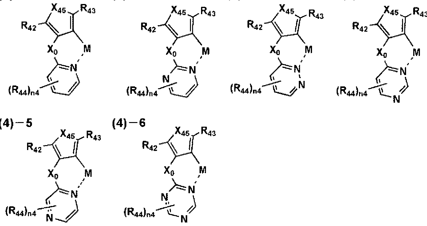 (
(
[0097] 一般式 (4) (4) 6において、 R 、 R は各々置換基を表し、 R は水素原子 [0097] In the general formulas (4) and (4) 6, R 1 and R 2 each represents a substituent, and R 1 represents a hydrogen atom.
42 44 43 42 44 43
または置換基を表す。 n4は 0〜2から選ばれる整数を表す。 X は 0、 S、 SOまたは S Or represents a substituent. n4 represents an integer selected from 0 to 2. X is 0, S, SO or S
45 45
Oを表す。 Xは 0、 S、 CH、 CHR、 C (R) 、 NR、 PR、 Si (R) 、 C = 0、 C = NR、 S Represents O. X is 0, S, CH, CHR, C (R), NR, PR, Si (R), C = 0, C = NR, S
2 0 2 2 2 2 0 2 2 2
0、 SOを表す。 Rはアルキル基、シクロアルキル基、ァルケ-ル基、ァリール基、複 0, represents SO. R represents an alkyl group, a cycloalkyl group, an alkyl group, an aryl group, a double group
2 2
素環基または芳香族複素環基を表す。 Mは元素周期表における第 8族〜第 10族の 金属元素を表す。 Represents a unicyclic group or an aromatic heterocyclic group. M represents a metal element of Group 8 to Group 10 in the periodic table.
[0098] R 、 R 、 R が表す置換基としては、前記一般式(1)の R、 R が表す置換基と同 [0098] The substituents represented by R 1, R 2 and R 3 are the same as the substituents represented by R and R in the general formula (1).
42 44 43 1 11 42 44 43 1 11
様のものが挙げられる。 Rの具体的基は前記一般式(3)の Rと同様のものが挙げられ る。 Something like that. Specific examples of R include the same groups as R in the general formula (3).
[0099] また、前記一般式 (4)で表される部分構造力 前記一般式(9B)または一般式(10 [0099] Further, the partial structural force represented by the general formula (4) The general formula (9B) or the general formula (10
B)で表される部分構造であることが好ま 、。 It is preferable that the partial structure represented by B).
[0100] 前記一般式(9B)または一般式(10B)において、 X 、 X 、 X 、 X は各々炭素原 [0100] In the general formula (9B) or the general formula (10B), X 1, X 2, X 3 and X 5 are each a carbon atom.
71 72 73 74 71 72 73 74
子または窒素原子を表し、 Qは炭素原子、 X 、 X と共に 6員の芳香族複素環を形 Represents a child atom or a nitrogen atom, Q forms a 6-membered aromatic heterocycle with carbon atom, X and X
3 71 72 3 71 72
成する原子群を表し、 Q Q
4は炭素原子、 X 、 X 4 is a carbon atom, X, X
73 74、窒素原子と共に 6員の芳香族複素 環を形成する原子群を表す。 X、 X 0 O す。 R 73 74 represents a group of atoms that together with the nitrogen atom form a 6-membered aromatic heterocycle. X, X 0 O R
3 4は 、 S、 S または SO 3 4 is S, S or SO
2を表 35は置換基を 表し、 R は水素原子または置換基を表す。 R 、 R 、 R 、 R はファンデルワールス In Table 35, 2 represents a substituent, and R represents a hydrogen atom or a substituent. R, R, R, R are van der Waals
46 36 37 45 47 46 36 37 45 47
体積が 20A3以上である置換基を表す。 n71、 n72、 n73は 0または 1を表す。但し、 n71 +n72≥lである。 Xは 0、 S、 CH、 CHR、 C (R) 、 NR、 PR、 Si (R) 、 C = 0、 Represents a substituent having a volume of 20A 3 or more. n71, n72, and n73 represent 0 or 1. However, n71 + n72≥l. X is 0, S, CH, CHR, C (R), NR, PR, Si (R), C = 0,
0 2 2 2 0 2 2 2
C =NR、 SO、 SOを表す。 Rはアルキル基、シクロアルキル基、ァルケ-ル基、ァリ
ール基、複素環基または芳香族複素環基を表す。 Mは元素周期表における第 8族 〜第 10族の金属元素を表す。 C represents NR, SO, SO. R represents an alkyl group, a cycloalkyl group, an alkyl group, an alkyl Represents an aryl group, a heterocyclic group or an aromatic heterocyclic group. M represents a metal element of Group 8 to Group 10 in the periodic table.
[0101] R 、R が表す置換基としては、前記一般式(1)の R、R が表す置換基と同様のも [0101] The substituents represented by R 1 and R 2 are the same as the substituents represented by R 1 and R 2 in the general formula (1).
35 46 1 11 35 46 1 11
のが挙げられる。 6員の芳香族複素環、ファンデルワールス体積については、前記一 般式 (7B)または一般式 (8B)におけるそれらと同様である。 Rの具体的基は前記一 般式(3)の Rと同様のものが挙げられる。 Can be mentioned. The 6-membered aromatic heterocycle and van der Waals volume are the same as those in the general formula (7B) or the general formula (8B). Specific examples of R include the same groups as R in the general formula (3).
[0102] 本発明に係るオルトメタル錯体として好ま ヽものは、前記一般式 (Z)で表される部 分構造が持つ配位子と共に、マイナス 1価のァ-オン性の単座配位子、マイナス 1価 の二座配位子、無電荷の単座配位子、無電荷の二座配位子が挙げられ、特に、マイ ナス 1価のァ-オン性の単座配位子と組み合わせて無電荷の単座配位子を用いるこ とが好まし 、。マイナス 1価のァ-オン性の単座配位子と組み合わせて用いるのが好 まし 、無電荷の単座配位子としては、後述の無電荷の単座配位子が挙げられる。 [0102] Preferred orthometal complexes according to the present invention include a minus monovalent monodentate ligand together with a ligand having a partial structure represented by the general formula (Z), Negative monovalent bidentate ligands, uncharged monodentate ligands, and uncharged bidentate ligands, especially in combination with negative monovalent terionic monodentate ligands. It is preferred to use a monodentate ligand of charge. It is preferably used in combination with a minus monovalent terionic monodentate ligand. Examples of the uncharged monodentate ligand include the below-mentioned uncharged monodentate ligand.
[0103] (マイナス 1価のァ-オン性の単座配位子) [0103] (minus monovalent terion monodentate ligand)
本発明においては、オルトメタル錯体力 下記に示す A群から選択されるァ-オン 性の単座配位子を有することが好まし 、。 In the present invention, it is preferable to have a monodentate ligand having an ionic nature selected from group A shown below.
[0104] [化 16]
[0104] [Chemical 16]
Br Br

~ S - ei C≡C— 6i ~ S- ei C≡C— 6 i

[0105] 上記 A郡において、 R はアルキル基、シクロアルキル基、ァリール基、複素環基ま [0105] In the above A group, R is an alkyl group, a cycloalkyl group, an aryl group, a heterocyclic group.
61 61
たは芳香族複素環基を表す。 R は置換基を表し、 n8は 0 3から選ばれる整数を表 Or represents an aromatic heterocyclic group. R represents a substituent, and n8 represents an integer selected from 0 to 3.
62 62
す。 The
[0106] R の具体的基は、前記一般式(3)のアルケニル基を除く Rと同様のものが挙げら [0106] Specific examples of R 1 include the same groups as R except for the alkenyl group of the general formula (3).
61 61
れる。 R が表す置換基としては、前記一般式(1)の R R が表す置換基と同様のも It is. The substituent represented by R 1 is the same as the substituent represented by R R in the general formula (1).
62 1 11 62 1 11
のが挙げられる。 Can be mentioned.
[0107] (マイナス 1価の二座配位子) [0107] (minus monovalent bidentate ligand)
本発明においては、オルトメタル錯体力 下記に挙げた部分構造カゝら選ばれるマイ ナス 1価の二座配位子を有することが好ましい。 In the present invention, it is preferable to have a negative monovalent bidentate ligand selected from the following partial structures.
[0108] [化 17]
[0108] [Chemical 17]
[8ΐ^ ] [6010] [8ΐ ^] [6010]

^ひ 0£/900Zdf/ェ:) d LZ 1^8£0I/900Z OAV
, ' ', ^^ 0 £ / 900Zdf / e :) d LZ 1 ^ 8 £ 0I / 900Z OAV , '',
,-<¾·,-<¾ ·
' '
' - s ' -s
Nへ To N
、Ο
 R , Ο R
ノ RM No R M
ン一 One
O O
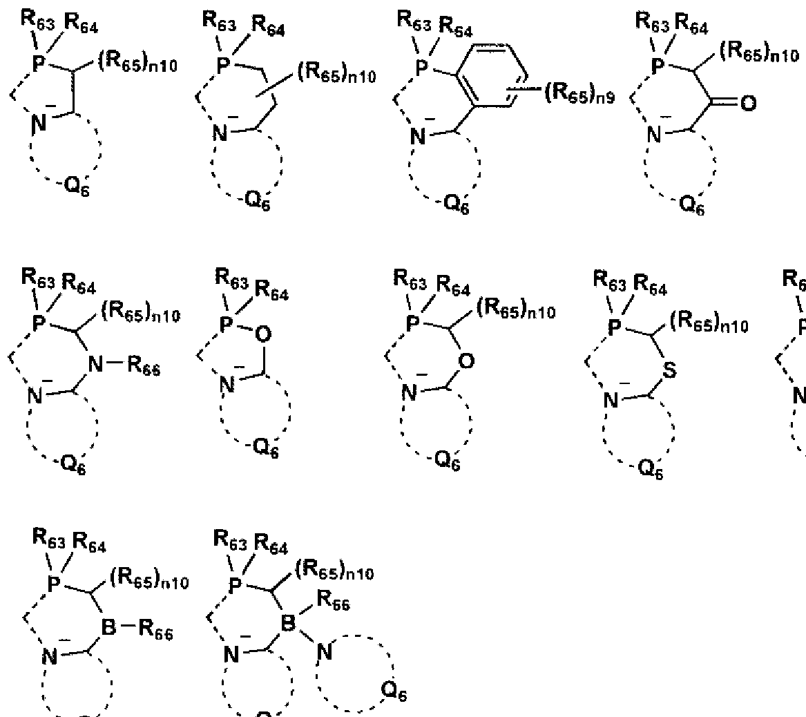
[0110] 上記各二座配位子において、 R 、 R 、 R はそれぞれアルキル基、シクロアルキル 基、ァリール基、複素環基または芳香族複素環基を表す。 R は置換基を表し、 n9は[0110] In each of the above bidentate ligands, R 1, R 2 and R 3 each represents an alkyl group, a cycloalkyl group, an aryl group, a heterocyclic group or an aromatic heterocyclic group. R represents a substituent, and n9 represents
0〜3の整数を表し、 nlOは 0〜2の整数を表す。 R は R —CO—または R —SO を表し、 R はアルキル基、シクロアルキル基、ァリール基、複素環基または芳香族 複素環基を表す。 Qは炭素、窒素と共に 5〜6員の芳香族複素環を形成する。 Qは 炭素、窒素と共に 5員の芳香族複素環を形成する。 N1 represents an integer of 0 to 3, and nlO represents an integer of 0 to 2. R represents R—CO— or R—SO, and R represents an alkyl group, a cycloalkyl group, an aryl group, a heterocyclic group or an aromatic heterocyclic group. Q forms a 5- to 6-membered aromatic heterocycle with carbon and nitrogen. Q forms a 5-membered aromatic heterocycle with carbon and nitrogen.
[0111] 上記のマイナス 1価のァ-オン性の二座配位子において、 R 、 R 、 R はアルキル
基、シクロアルキル基、ァリール基、複素環基または芳香族複素環基を表す。 R は [0111] In the minus monovalent terion bidentate ligand, R 1, R 2 and R 3 are alkyls. Represents a group, a cycloalkyl group, an aryl group, a heterocyclic group or an aromatic heterocyclic group. R is
65 置換基を表し、 n9は 0〜3の整数を表し、 nlOは 0〜2の整数を表す。 R は R —CO 65 represents a substituent, n9 represents an integer of 0 to 3, and nlO represents an integer of 0 to 2. R is R —CO
67 68 または R —SO—を表し、 R はアルキル基、シクロアルキル基、ァリール基、複素 67 68 or R —SO—, where R is an alkyl group, cycloalkyl group, aryl group, complex
68 2 68 68 2 68
環基または芳香族複素環基を表す。 Qは炭素、窒素と共に 5〜6員の芳香族複素環 Represents a cyclic group or an aromatic heterocyclic group. Q is a 5- or 6-membered aromatic heterocycle with carbon and nitrogen
5 Five
を形成する。 Qは炭素、窒素と共に 5員の芳香族複素環を形成する。 Form. Q forms a 5-membered aromatic heterocycle with carbon and nitrogen.
6 6
[0112] R 、R 、R 、R の具体的基は前記一般式(3)のアルケニル基を除く Rと同様のも [0112] Specific groups of R 1, R 2, R 3 and R 4 are the same as those of R except for the alkenyl group of the general formula (3).
63 64 66 68 63 64 66 68
のが挙げられる。 R が表す置換基としては、前記一般式(1)の R、R が表す置換基 Can be mentioned. As the substituent represented by R 1, the substituent represented by R and R 1 in the general formula (1)
65 1 11 65 1 11
と同様のものが挙げられる。 Qは一般式(8)の Qと同義である。 Qとしてはピロール The same thing is mentioned. Q is synonymous with Q in formula (8). Q as pyrrole
5 2 6 5 2 6
環、トリアジン環、イミダゾール環、ピラゾール環、トリァゾール環等が挙げられる。 Ring, triazine ring, imidazole ring, pyrazole ring, triazole ring and the like.
[0113] (無電荷の二座配位子) [0113] (Uncharged bidentate ligand)
本発明においては、オルトメタル錯体力 下記に挙げた部分構造カゝら選ばれる無 電荷の二座配位子を有することが好ま 、。 In the present invention, it is preferable to have an uncharged bidentate ligand selected from the following partial structure groups.
[0114] [化 19]
[0114] [Chemical 19]


[0117] 上記の各無電荷の二座配位子において、 R 、R 、R 、R 、R 、R 、R 、R 、R [0117] In each of the above uncharged bidentate ligands, R 1, R 2, R 3, R 4, R 5, R 5, R 5, R 6, R 5
71 72 79 81 82 86 87 88 8 R R R R はアルキル基、シクロアルキル基、ァリール基、複素環基または 71 72 79 81 82 86 87 88 8 R R R R represents an alkyl group, a cycloalkyl group, an aryl group, a heterocyclic group or
9 95 96 97 98 9 95 96 97 98
芳香族複素環基を表す。 R 、R 、R 、R 、R 、R 、R 、R 、R 、R 、R 、R Represents an aromatic heterocyclic group. R, R, R, R, R, R, R, R, R, R, R, R
73 74 76 77 78 83 84 90 92 93 99 A1は 置換基を表し、 R R R R R R は水素原子または置換基を表す。 nilは 73 74 76 77 78 83 84 90 92 93 99 A1 represents a substituent, and R R R R R R represents a hydrogen atom or a substituent. nil
75 80 85 91 94 AO 75 80 85 91 94 AO
0 2の整数を表し、 nl2は 0 3の整数を表す。 nl3は 0 4の整数を表す。 nl4 n 15は 0 3の整数を表し、 nl6は 0 2の整数を表す。 nl7は 0 2の整数を表し、 nl 8は 0 3の整数を表す。 nl9は 0 4の整数を表す。 n20 n22は 0 2の整数を表 し、 n21は 0 4の整数を表す。 n23は 0 2の整数を表し、 n24は 0 4の整数を表 す。 Q Q Q Q 員の 0 2 represents an integer, and nl2 represents an integer of 0 3. nl3 represents an integer of 0 4. nl4 n 15 represents an integer of 0 3, and nl6 represents an integer of 0 2. nl7 represents an integer of 0 2 and nl 8 represents an integer of 0 3. nl9 represents an integer of 04. n20 n22 represents an integer of 0 2 and n21 represents an integer of 0 4. n23 represents an integer of 0 2 and n24 represents an integer of 0 4. Q Q Q Q
10 11 12 13は炭素、窒素と共に 5 6 芳香族複素環を形成する原子 群を表す。 10 11 12 13 represents an atomic group forming a 5 6 aromatic heterocycle with carbon and nitrogen.
[0118] 上記の各無電荷の二座配位子において、 R R R R R R R R R [0118] In each of the above uncharged bidentate ligands, R R R R R R R R R
71 72 79 81 82 86 87 88 8 R R R R の具体的基は、前記一般式(3)のァルケ-ル基を除く Rと同様の 71 72 79 81 82 86 87 88 8 R R R The specific group of R is the same as R except for the alkenyl group of the general formula (3).
9 95 96 97 98 9 95 96 97 98
ものが挙げられる。 R 、R 、R 、R 、R 、R 、R 、R 、R 、R 、R 、R 、R 、R Things. R, R, R, R, R, R, R, R, R, R, R, R, R, R
73 74 76 77 78 83 84 86 90 92 93 99 A1 75 R R R R R が表す置換基としては、前記一般式(1)の R R が表す置 73 74 76 77 78 83 84 86 90 92 93 99 A1 75 R R R R R represents a substituent represented by R R in the general formula (1).
80 85 91 94 80 85 91 94
換基と同様のものが挙げられる。 Q Q Q Q は一般式 (8)の Qと同義である。 The thing similar to a substituent is mentioned. Q Q Q Q is synonymous with Q in general formula (8).
[0119] 力かる無電荷の二座配位子と組み合わせて用いるのが好ましいマイナス 1価のァ-
オンとしては、以下のものが挙げられる [0119] It is preferable to use in combination with a strong uncharged bidentate ligand. On includes the following:
[0120] [化 22] [0120] [Chemical 22]
CI Br CI Br
0 0 0 0
一 // ― // 一 One // ― // One
o-c s-c s— c o-c s-c s— c
\ \ \ \ \ \
0 0 0 0
一 t - + - + One t-+-+
0-S"RA8 0-S-RA8 0-S "R A8 0-SR A8
τ τ
ο ο
o ο o ο
-牛 -Cow
0-ΒΓ-*-0 0-ΒΓ-*-0
+ 一 + One
0 ο 0 ο
1一 1
-B-F -B -R -B-F -B -R
! !
^B2 ^ B2
[0121] 式中、 R はアルキル基、シクロアルキル基、ァリール基、複素環基または芳香族複 [0121] In the formula, R represents an alkyl group, a cycloalkyl group, an aryl group, a heterocyclic group, or an aromatic compound.
A8 A8
素環基を表す。 R R Represents a ring group. R R
A9、R A9, R
B0、 Bl、R B0, Bl, R
B2はァリール基または芳香族複素環基を表す。 B2 represents an aryl group or an aromatic heterocyclic group.
[0122] R の具体的基は前記一般式(3)のアルケニル基を除く Rと同様のものが挙げられ [0122] Specific examples of R include the same groups as R except for the alkenyl group of the general formula (3).
A8 A8
る。 R 、R 、R 、R の具体的基は前記一般式 (3)のァリール基、芳香族複素環基 The Specific groups for R 1, R 2, R 3, and R 4 are aryl groups and aromatic heterocyclic groups in the general formula (3).
A9 B0 Bl B2 A9 B0 Bl B2
で挙げられている。 It is mentioned in.
[0123] (無電化の単座配位子) [0123] (Electrically electrified monodentate ligand)
本発明にお ヽては、オルトメタル錯体が下記に示す B群カゝら選択される無電荷の配 位子の 、ずれかを有することが好まし 、。 In the present invention, it is preferable that the ortho metal complex has any one of the following uncharged ligands selected from the group B group.
[0124] [化 23]
B群: [0124] [Chemical 23] Group B:
N≡C-— ft2 -N≡C-0- A2 - N≡C— S— RA - -
 N N≡C-- ft2 -N≡C-0- A2 - N≡C- S- R A - - N
-N -N (RM)N " "r- (f¾A4)n25 -N -N (R M ) N "" r- (f¾A4) n25

[0125] 上記 B郡において、 R 、R 、R 、R 、R はアルキル基、シクロアルキル基、ァリ [0125] In the above-mentioned B group, R 1, R 2, R 3, R 4, R 5 are an alkyl group, a cycloalkyl group, an aryl group
A2 A3 A5 A6 A7 A2 A3 A5 A6 A7
ール基、複素環基または芳香族複素環基を表す。 R は置換基を表し、 n25は 0〜2 Represents an aryl group, a heterocyclic group or an aromatic heterocyclic group. R represents a substituent, and n25 represents 0 to 2
A4 A4
から選ばれる整数を表す。 R 、R 、R 、R 、R の具体的基は、前記一般式(3)の Represents an integer selected from Specific groups of R 1, R 2, R 3, R 4, and R 5 are represented by the general formula (3).
A2 A3 A5 A6 A7 A2 A3 A5 A6 A7
ァルケ-ル基を除く Rと同様のものが挙げられる。 R が表す置換基としては、前記一 Examples are the same as R except for the alkenyl group. As the substituent represented by R 1,
A4 A4
般式(1)の R、 R が表す置換基と同様のものが挙げられる。 Examples thereof are the same as the substituents represented by R and R in the general formula (1).
1 11 1 11
[0126] 以下、本発明に好ましく用いられるオルトメタル錯体を示す。 [0126] Ortho metal complexes preferably used in the present invention are shown below.
[0127] [化 24]
[S2^ ] [82 TO] [0127] [Chemical 24] [S2 ^] [82 TO]


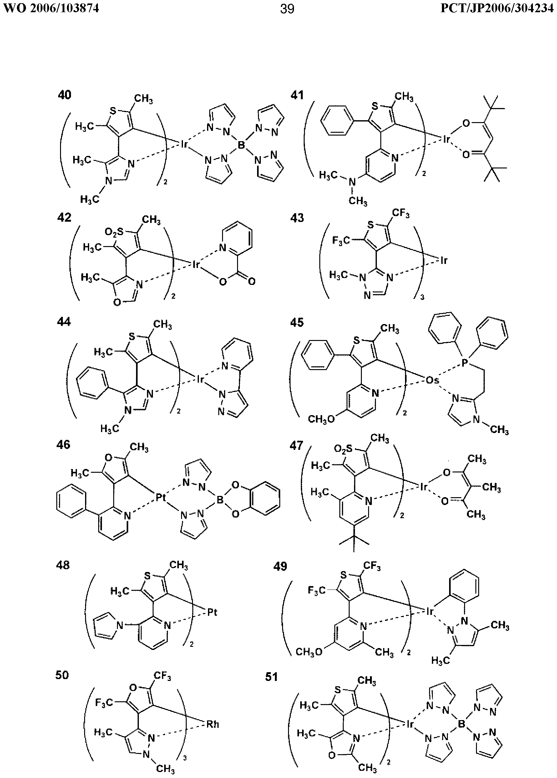
[0132] [化 29]
[0132] [Chemical 29]
[οε^] [εειο] [οε ^] [εειο]


[0134] [化 31]
[0134] [Chemical 31]

[0135] [化 32]
[εε^ ] [9ε TO] [0135] [Chemical 32] [εε ^] [9ε TO]


[0137] [化 34]
[0137] [Chemical 34]

[0139] 《有機 EL素子材料の有機 EL素子への適用》 [0139] <Application of organic EL element materials to organic EL elements>
本発明において、上記有機 EL素子材料を含有する有機 EL素子とは、有機 EL素 子材料が有機 EL素子を構成する ヽずれかの有機層を形成するか、または有機層に 含有された有機 EL素子を表す。 In the present invention, the organic EL element containing the above organic EL element material means that the organic EL element material forms any organic layer constituting the organic EL element or the organic EL contained in the organic layer. Represents an element.
[0140] 本発明の有機 EL素子材料を有機 EL素子に適用する際、有機 EL素子の構成層の 少なくとも 1層に含有することを特徴とし、また構成層として発光層を有し、該発光層 に本発明の有機エレクト口ルミネッセンス素子材料を含有することを特徴とする。また 、構成層として正孔阻止層を有し、該正孔阻止層に本発明の有機エレクト口ルミネッ センス素子材料を含有することが好ましい。また、構成層の少なくとも一層にカルバゾ ール誘導体を含有することが好まし ヽ。 [0140] When the organic EL device material of the present invention is applied to an organic EL device, it is contained in at least one of the constituent layers of the organic EL device, and has a light emitting layer as a constituent layer, and the light emitting layer It contains the organic electoluminescence device material of the present invention. Moreover, it is preferable to have a hole blocking layer as a constituent layer and to contain the organic electoluminescence device material of the present invention in the hole blocking layer. In addition, it is preferable that at least one of the constituent layers contains a carbazole derivative.
[0141] 本発明の有機 EL素子材料を用いて、有機 EL素子を作製する場合、有機 EL素子 の構成層(詳細は後述する)の中で、発光層または正孔阻止層に用いることが好まし い。また、発光層中では上記のように、発光ドーパントとして好ましく用いられる。 [0141] When an organic EL element is produced using the organic EL element material of the present invention, it is preferably used for a light emitting layer or a hole blocking layer in the constituent layers (details will be described later) of the organic EL element. Good. In the light emitting layer, as described above, it is preferably used as a light emitting dopant.
[0142] (発光ホストと発光ドーパント) [0142] (Light emitting host and light emitting dopant)
発光層中の主成分であるホストイ匕合物である発光ホストに対する発光ドーパントとの 混合比は好ましくは質量で 0. 1〜30質量%未満の範囲に調整することである。 The mixing ratio of the light-emitting dopant to the light-emitting host that is the host compound as the main component in the light-emitting layer is preferably adjusted to a range of 0.1 to less than 30% by mass.
[0143] 但し、発光ドーパントは複数種の化合物を混合して用いてもよぐ混合する相手は 構造を異にする、その他の金属錯体やその他の構造を有するリン光性ドーパントや 蛍光性ドーパントでもよい。 [0143] However, the luminescent dopant may be a mixture of a plurality of types of compounds. The mixed partner may have a different structure, and other metal complexes or phosphorescent dopants or fluorescent dopants having other structures may be used. Good.
[0144] ここで、発光ドーパントとして用いられる白金錯体と併用してもよいドーパント(リン光 性ドーパント、蛍光性ドーパント等)について述べる。発光ドーパントは、大きくわけて 、蛍光を発光する蛍光性ドーパントとリン光を発光するリン光性ドーパントの 2種類が ある。 [0144] Here, dopants (phosphorescent dopant, fluorescent dopant, etc.) that may be used in combination with the platinum complex used as the luminescent dopant will be described. The light-emitting dopant is roughly classified into two types: a fluorescent dopant that emits fluorescence and a phosphorescent dopant that emits phosphorescence.
[0145] 前者 (蛍光性ドーパント)の代表例としては、クマリン系色素、ピラン系色素、シ了ニ ン系色素、クロコニゥム系色素、スクァリウム系色素、ォキソベンツアントラセン系色素 、フルォレセイン系色素、ローダミン系色素、ピリリウム系色素、ペリレン系色素、スチ ルベン系色素、ポリチォフェン系色素、または希土類錯体系蛍光体等が挙げられる。
[0146] 後者 (リン光性ドーパント)の代表例としては、好ましくは元素の周期表で 8属、 9属、 10属の金属を含有する錯体系化合物であり、更に好ましくはイリジウム化合物、ォス ミゥム化合物であり、中でも最も好ま U、のはイリジウム化合物である。 [0145] Typical examples of the former (fluorescent dopant) include coumarin dyes, pyran dyes, cinine dyes, croconium dyes, squalium dyes, oxobenzanthracene dyes, fluorescein dyes, rhodamines. And dyes such as a dye, a pyrylium dye, a perylene dye, a stilbene dye, a polythiophene dye, or a rare earth complex phosphor. [0146] As a typical example of the latter (phosphorescent dopant), a complex compound containing a metal belonging to Group 8, Group 9, or Group 10 in the periodic table of elements is preferable, and an iridium compound or a phosphine is more preferable. Of these, the most preferred U is iridium compounds.
[0147] 具体的には以下の特許公報に記載されている化合物である。 [0147] Specifically, it is a compound described in the following patent publications.
[0148] 国際公開第 OOZ70655号パンフレツ K特開 2002— 280178号公報、特開 2001[0148] International Publication No. OOZ70655 Pamphlet K JP 2002-280178 A, JP 2001
— 181616号公報、特開 2002— 280179号公報、特開 2001— 181617号公報、 特開 2002— 280180号公報、特開 2001— 247859号公報、特開 2002— 299060 号公報、特開 2001— 313178号公報、特開 2002— 302671号公報、特開 2001— 345183号公報、特開 2002— 324679号公報、国際公開第 02,15645号パンフ レッド、特開 2002— 332291号公報、特開 2002— 50484号公報、特開 2002— 33 2292号公報、特開 2002— 83684号公報、特表 2002— 540572号公報、特開 20 02— 117978号公報、特開 2002— 338588号公報、特開 2002— 170684号公報 、特開 2002— 352960号公報、国際公開第 01/93642号パンフレット、特開 2002— No. 181616, No. 2002-280179, No. 2001-181617, No. 2002-280180, No. 2001-247859, No. 2002-299060, No. 2001-313178 JP, JP 2002-302671, JP 2001-345183, JP 2002-324679, WO 02,15645 Pamphlet, JP 2002-332291, JP 2002-50484 No., JP 2002-33 2292, JP 2002-83684, JP 2002-540572, JP 20 02-117978, JP 2002-338588, JP 2002-170684 No., JP 2002-352960 A, WO 01/93642 pamphlet, JP 2002
— 50483号公報、特開 2002— 100476号公報、特開 2002— 173674号公報、特 開 2002— 359082号公報、特開 2002— 175884号公報、特開 2002— 363552号 公報、特開 2002— 184582号公報、特開 2003— 7469号公報、特表 2002— 525 808号公報、特開 2003— 7471号公報、特表 2002— 525833号公報、特開 2003— 50483, JP 2002-100476, JP 2002-173674, JP 2002-359082, JP 2002-175884, JP 2002-363552, JP 2002-184582 Publication, JP 2003-7469, JP 2002-525 808, JP 2003-7471, JP 2002-525833, JP 2003
— 31366号公報、特開 2002— 226495号公報、特開 2002— 234894号公報、特 開 2002— 235076号公報、特開 2002— 241751号公報、特開 2001— 319779号 公報、特開 2001— 319780号公報、特開 2002— 62824号公報、特開 2002— 10 0474号公報、特開 2002— 203679号公報、特開 2002— 343572号公報、特開 2 002— 203678号公報等。 — 31366, JP 2002-226495, JP 2002-234894, JP 2002-235076, JP 2002-241751, JP 2001-319779, JP 2001-319780 JP, 2002-62824, JP 2002-10474, JP 2002-203679, JP 2002-343572, JP 2002-203678, and the like.
[0149] 本発明に係る上記オルトメタル錯体と併用が好まし!/ヽ金属錯体を下記に示す。 [0149] The ortho metal complex according to the present invention is preferably used in combination with the above-mentioned ortho metal complex!
[0150] [化 35]
lr-1 lr-2 [0150] [Chemical 35] lr-1 lr-2


発光ホスト(単にホストとも!、う)とは、 2種以上の化合物で構成される発光層中にて 混合比 (質量)の最も多い化合物のことを意味し、それ以外の化合物については「ド 一パント化合物(単に、ドーパントともいう)」という。例えば、発光層をィ匕合物 A、化合 物 Bという 2種で構成し、その混合比が A:B= 10 :90であれば化合物 Aがドーパント 化合物であり、化合物 Bがホストイ匕合物である。更に発光層をィ匕合物 A、化合物 B、 化合物 Cの 3種力 構成し、その混合比が八^:じ=5:10:85でぁれば、化合物 A、
化合物 Bがドーパント化合物であり、化合物 Cがホストイ匕合物である。 The light-emitting host (simply referred to as “host”!) Means the compound with the highest mixing ratio (mass) in the light-emitting layer composed of two or more types of compounds. One pant compound (also simply referred to as dopant) ". For example, if the light emitting layer is composed of two compounds A and B and the mixing ratio is A: B = 10: 90, compound A is a dopant compound and compound B is a host compound. It is. Furthermore, if the light emitting layer is composed of three compounds A, Compound B, and Compound C, and the mixing ratio is 8 ^: 5 = 10: 85, then Compound A, Compound B is a dopant compound and Compound C is a host compound.
[0153] 本発明に用いられる発光ホストとしては、併用される発光ドーパントのリン光 0— 0バ ンドよりも短波長なそれをもつ化合物が好ましぐ発光ドーパントにそのリン光 0— 0バ ンドが 480nm以下である青色の発光成分を含む化合物を用いる場合には、発光ホ ストとしてはリン光 0— 0バンドが 450nm以下であることが好ましい。 [0153] As the luminescent host used in the present invention, a compound having a shorter wavelength than the phosphorescent 0-0 band of the luminescent dopant used in combination is preferably used as the luminescent dopant. When a compound containing a blue light-emitting component having a wavelength of 480 nm or less is used, the phosphorescent 0-0 band is preferably 450 nm or less as the light-emitting host.
[0154] 本発明に係る発光ホストとしては、構造的には特に制限はないが、代表的にはカル バゾール誘導体、トリアリールァミン誘導体、芳香族ボラン誘導体、含窒素複素環化 合物、チォフェン誘導体、フラン誘導体、オリゴァリーレン化合物等の基本骨格を有 し、且つ前記 0— 0バンド力 50nm以下の化合物が好ましい化合物として挙げられる 。また、本発明に係る発光ホストは低分子化合物でも、繰り返し単位をもつ高分子化 合物でもよぐビニル基やエポキシ基のような重合性基を有する低分子化合物 (蒸着 重合性発光ホスト)でも 、 、。 [0154] The luminescent host according to the present invention is not particularly limited in terms of structure, but is typically a carbazole derivative, a triarylamine derivative, an aromatic borane derivative, a nitrogen-containing heterocyclic compound, thiophene. Preferred compounds include those having a basic skeleton such as derivatives, furan derivatives and oligoarylene compounds and having the 0-0 band force of 50 nm or less. In addition, the light emitting host according to the present invention may be a low molecular compound, a high molecular compound having a repeating unit, or a low molecular compound having a polymerizable group such as a vinyl group or an epoxy group (evaporation polymerizable light emitting host). ,,.
[0155] 発光ホストとしては、正孔輸送能、電子輸送能を有しつつ、且つ発光の長波長化を 防ぎ、なお且つ高 Tg (ガラス転移温度)である化合物が好ま 、。 [0155] As the light-emitting host, a compound that has a hole transporting ability and an electron transporting ability, prevents an increase in the wavelength of light emission, and has a high Tg (glass transition temperature) is preferable.
[0156] 発光ホストの具体例としては、以下の文献に記載されている化合物が好適である。 [0156] As specific examples of the luminescent host, compounds described in the following documents are suitable.
例えば、特開 2001— 257076号公報、特開 2002— 308855号公報、特開 2001— 313179号公報、特開 2002— 319491号公報、特開 2001— 357977号公報、特 開 2002— 334786号公報、特開 2002— 8860号公報、特開 2002— 334787号公 報、特開 2002— 15871号公報、特開 2002— 334788号公報、特開 2002— 4305 6号公報、特開 2002— 33 9号公報、特開 2002— 75645号公報、特開 2002— 338579号公報、特開 2002— 105445号公報、特開 2002— 343568号公報、特 開 2002— 141173号公報、特開 2002— 352957号公報、特開 2002— 203683号 公報、特開 2002— 363227号公報、特開 2002— 231453号公報、特開 2003— 3 165号公報、特開 2002— 234888号公報、特開 2003— 27048号公報、特開 200 2— 255934号公報、特開 2002— 260861号公報、特開 2002— 280183号公報、 特開 2002— 299060号公報、特開 2002— 302516号公報、特開 2002— 305083 号公報、特開 2002— 305084号公報、特開 2002— 308837号公報等。 For example, JP 2001-257076, JP 2002-308855, JP 2001-313179, JP 2002-319491, JP 2001-357977, JP 2002-334786, JP 2002-8860, JP 2002-334787, JP 2002-15871, JP 2002-334788, JP 2002-4305 6, JP 2002-339 JP, 2002-75645, JP 2002-338579, JP 2002-105445, JP 2002-343568, JP 2002-141173, JP 2002-352957, JP JP 2002-203683, JP 2002-363227, JP 2002-231453, JP 2003-3165, JP 2002-234888, JP 2003-27048, JP 200 2-255934, JP 2002-260861, JP 2002-280183, JP 2002-299060, JP 2002-302516, JP 2002-305083 JP 2002- 305084, JP-A No. 2002- 308837 Publication.
[0157] 次に、代表的な有機 EL素子の構成について述べる。
[0158] 《有機 EL素子の構成層》 Next, the configuration of a typical organic EL element will be described. [0158] <Structure layer of organic EL element>
本発明の有機 EL素子の構成層につ 、て説明する。 The constituent layers of the organic EL device of the present invention will be described.
[0159] 本発明の有機 EL素子の層構成の好ましい具体例を以下に示すが、本発明はこれ らに限定されない。 [0159] Preferred specific examples of the layer structure of the organic EL device of the present invention are shown below, but the present invention is not limited thereto.
[0160] (i)陽極 Z発光層 Z電子輸送層 Z陰極 [0160] (i) Anode Z light emitting layer Z electron transport layer Z cathode
(ii)陽極 Z正孔輸送層 Z発光層 Z電子輸送層 Z陰極 (ii) Anode Z hole transport layer Z light emitting layer Z electron transport layer Z cathode
(iii)陽極 Z正孔輸送層 Z発光層 Z正孔阻止層 Z電子輸送層 Z陰極 (iii) Anode Z hole transport layer Z light emitting layer Z hole blocking layer Z electron transport layer Z cathode
(iv)陽極 Z正孔輸送層 Z発光層 Z正孔阻止層 Z電子輸送層 Z陰極バッファ一層 Z陰極 (iv) Anode Z hole transport layer Z light emitting layer Z hole blocking layer Z electron transport layer Z cathode buffer layer Z cathode
(v)陽極 Z陽極バッファ一層 Z正孔輸送層 Z発光層 Z正孔阻止層 Z電子輸送層 Z陰極バッファ一層 Z陰極 (v) Anode Z anode buffer layer Z hole transport layer Z light emitting layer Z hole blocking layer Z electron transport layer Z cathode buffer layer Z cathode
《発光層》 <Light emitting layer>
本発明にお 、ては、本発明の有機 EL素子用材料は発光層にお 、て用いられるこ とが好まし 、が、これら以外にも上記のような公知の発光ホストや発光ドーパントを併 用してちょい。 In the present invention, the organic EL device material of the present invention is preferably used in the light emitting layer, but in addition to these, the above-mentioned known light emitting host and light emitting dopant are used together. Use it.
[0161] ここで、本発明に記載の効果 (発光輝度の向上、発光寿命の長寿命化)を更に向 上させる観点から、発光層が下記一般式 (A)で表される化合物を含有することが好 ま 、。これらの化合物は発光層にお 、て発光ホストとして好ましく用いられる。 [0161] Here, from the viewpoint of further improving the effects described in the present invention (improvement of light emission luminance, prolongation of light emission lifetime), the light emitting layer contains a compound represented by the following general formula (A). I like it. These compounds are preferably used as a light emitting host in the light emitting layer.
[0162] [化 37] [0162] [Chemical 37]
-般式 (A) -General formula (A)
^101 i \ I Z2 ^ 101 i \ IZ 2
、? -z3- - -c ,? -z 3 ---c
[0163] 上記一般式 (A)において、 Zは置換基を有してもよい芳香族複素環を形成する原 [0163] In the above general formula (A), Z is an element forming an aromatic heterocyclic ring which may have a substituent.
1 1
子群を表し、 zは置換基を有してもよい芳香族複素環、もしくは芳香族炭化水素環を Z represents an aromatic heterocycle or an aromatic hydrocarbon ring which may have a substituent.
2 2
形成する原子群を表し、 Zは 2価の連結基もしくは単なる結合手を表す。 R は水素 Represents the atomic group to be formed, Z represents a divalent linking group or a simple bond. R is hydrogen
3 101 原子、もしくは置換基を表す。
[0164] Z、 Zの原子群力 表される芳香族複素環としては、フラン環、チォフェン環、ピリRepresents 3 101 atoms or substituents. [0164] Aromatic heterocycles represented by the atomic group forces of Z and Z include furan rings, thiophene rings, and pyri rings.
1 2 1 2
ジン環、ピリダジン環、ピリミジン環、ピラジン環、トリアジン環、ベンゾイミダゾール環、 ォキサジァゾール環、トリァゾール環、イミダゾール環、ピラゾール環、チアゾール環、 インドール環、ベンゾイミダゾール環、ベンゾチアゾール環、ベンゾォキサゾール環、 キノキサリン環、キナゾリン環、フタラジン環、力ルバゾール環、カルボリン環、ジァザ 力ルバゾール環 (カルボリン環を構成する炭化水素環の炭素原子の一つが更に窒素 原子で置換されている環を示す)等が挙げられる。更に前記芳香族複素環は、後述 する R で表される置換基を有してもよい。 Gin ring, pyridazine ring, pyrimidine ring, pyrazine ring, triazine ring, benzimidazole ring, oxadiazole ring, triazole ring, imidazole ring, pyrazole ring, thiazole ring, indole ring, benzimidazole ring, benzothiazole ring, benzoxazole ring Quinoxaline ring, quinazoline ring, phthalazine ring, force rubazole ring, carboline ring, diaza force rubazole ring (showing a ring in which one of the carbon atoms of the hydrocarbon ring constituting the carboline ring is further substituted with a nitrogen atom), etc. Can be mentioned. Furthermore, the aromatic heterocyclic ring may have a substituent represented by R described later.
101 101
[0165] Zの原子群から表される芳香族炭化水素環としては、ベンゼン環、ビフエ-ル環、 [0165] The aromatic hydrocarbon ring represented by the atomic group of Z includes a benzene ring, a biphenyl ring,
2 2
ナフタレン環、ァズレン環、アントラセン環、フエナントレン環、ピレン環、タリセン環、 ナフタセン環、トリフエ-レン環、 o—テルフエ-ル環、 m—テルフエ-ル環、 p—テル フエ-ル環、ァセナフテン環、コロネン環、フルオレン環、フルオラントレン環、ナフタ セン環、ペンタセン環、ペリレン環、ペンタフェン環、ピセン環、ピレン環、ピラントレン 環、アンスラアントレン環等が挙げられる。更に前記芳香族炭化水素環は、後述する R で表される置換基を有してもよい。 Naphthalene ring, azulene ring, anthracene ring, phenanthrene ring, pyrene ring, taricene ring, naphthacene ring, triphenylene ring, o-terphel ring, m-terphel ring, p-terphenyl ring, and acenaphthene ring , Coronene ring, fluorene ring, fluoranthrene ring, naphthacene ring, pentacene ring, perylene ring, pentaphen ring, picene ring, pyrene ring, pyranthrene ring, anthraanthrene ring, and the like. Furthermore, the aromatic hydrocarbon ring may have a substituent represented by R 1 described later.
101 101
[0166] R で表される置換基としては、アルキル基(例えば、メチル基、ェチル基、プロピル [0166] Examples of the substituent represented by R include an alkyl group (for example, a methyl group, an ethyl group, a propyl group).
101 101
基、イソプロピル基、 tert—ブチル基、ペンチル基、へキシル基、ォクチル基、ドデシ ル基、トリデシル基、テトラデシル基、ペンタデシル基等)、シクロアルキル基 (例えば 、シクロペンチル基、シクロへキシル基等)、ァルケ-ル基 (例えば、ビュル基、ァリル 基等)、アルキニル基 (例えば、ェチニル基、プロパルギル基等)、ァリール基 (例えば Group, isopropyl group, tert-butyl group, pentyl group, hexyl group, octyl group, dodecyl group, tridecyl group, tetradecyl group, pentadecyl group, etc.), cycloalkyl group (for example, cyclopentyl group, cyclohexyl group, etc.) Alkenyl group (for example, buyl group, allyl group, etc.), alkynyl group (for example, ethynyl group, propargyl group, etc.), aryl group (for example,
、フエ-ル基、ナフチル基等)、芳香族複素環基 (例えば、フリル基、チェ-ル基、ピリ ジル基、ピリダジ -ル基、ピリミジ -ル基、ピラジュル基、トリアジニル基、イミダゾリル 基、ピラゾリル基、チアゾリル基、キナゾリ-ル基、フタラジニル基等)、複素環基 (例 えば、ピロリジル基、イミダゾリジル基、モルホリル基、ォキサゾリジル基等)、アルコキ シル基 (例えば、メトキシ基、エトキシ基、プロピルォキシ基、ペンチルォキシ基、へキ シルォキシ基、ォクチルォキシ基、ドデシルォキシ基等)、シクロアルコキシル基 (例 えば、シクロペンチルォキシ基、シクロへキシルォキシ基等)、ァリールォキシ基 (例え ば、フエノキシ基、ナフチルォキシ基等)、アルキルチオ基 (例えば、メチルチオ基、ェ
チルチオ基、プロピルチオ基、ペンチルチオ基、へキシルチオ基、ォクチルチオ基、 ドデシルチオ基等)、シクロアルキルチオ基 (例えば、シクロペンチルチオ基、シクロ へキシルチオ基等)、ァリールチオ基 (例えば、フエ-ルチオ基、ナフチルチオ基等) 、アルコキシカルボ-ル基(例えば、メチルォキシカルボ-ル基、ェチルォキシカルボ ニル基、ブチルォキシカルボ-ル基、ォクチルォキシカルボ-ル基、ドデシルォキシ カルボ-ル基等)、ァリールォキシカルボ-ル基(例えば、フエ-ルォキシカルボ-ル 基、ナフチルォキシカルボ-ル基等)、スルファモイル基(例えば、アミノスルホ -ル基 、メチルアミノスルホ -ル基、ジメチルアミノスルホ -ル基、ブチルアミノスルホ -ル基 、へキシルアミノスルホ -ル基、シクロへキシルアミノスルホ -ル基、ォクチルアミノス ルホ-ル基、ドデシルアミノスルホ-ル基、フエ-ルアミノスルホ -ル基、ナフチルアミ ノスルホ -ル基、 2—ピリジルアミノスルホ -ル基等)、ァシル基 (例えば、ァセチル基 、ェチルカルボ-ル基、プロピルカルボ-ル基、ペンチルカルボ-ル基、シクロへキ シルカルボ-ル基、ォクチルカルポ-ル基、 2—ェチルへキシルカルボ-ル基、ドデ シルカルボ-ル基、フ -ルカルポ-ル基、ナフチルカルボ-ル基、ピリジルカルボ -ル基等)、ァシルォキシ基 (例えば、ァセチルォキシ基、ェチルカルボニルォキシ 基、ブチルカルボ-ルォキシ基、ォクチルカルボ-ルォキシ基、ドデシルカルボ -ル ォキシ基、フエニルカルボ-ルォキシ基等)、アミド基 (例えば、メチルカルボ-ルアミ ノ基、ェチルカルボ-ルァミノ基、ジメチルカルボ-ルァミノ基、プロピルカルボ-ルァ ミノ基、ペンチルカルボ-ルァミノ基、シクロへキシルカルボ-ルァミノ基、 2—ェチル へキシルカルボ-ルァミノ基、ォクチルカルボ-ルァミノ基、ドデシルカルボ-ルァミノ 基、フ -ルカルポ-ルァミノ基、ナフチルカルボ-ルァミノ基等)、力ルバモイル基( 例えば、ァミノカルボ-ル基、メチルァミノカルボ-ル基、ジメチルァミノカルボ-ル基 、プロピルアミノカルボ-ル基、ペンチルァミノカルボ-ル基、シクロへキシルァミノ力 ルポ-ル基、ォクチルァミノカルボ-ル基、 2—ェチルへキシルァミノカルボ-ル基、 ドデシルァミノカルボ-ル基、フエ-ルァミノカルボ-ル基、ナフチルァミノカルボ-ル 基、 2—ピリジルァミノカルボニル基等)、ウレイド基 (例えば、メチルウレイド基、ェチ ルゥレイド基、ペンチルゥレイド基、シクロへキシルウレイド基、ォクチルゥレイド基、ド デシルゥレイド基、フ ニルゥレイド基ナフチルウレイド基、 2—ピリジルアミノウレイド
基等)、スルフィエル基(例えば、メチルスルフィ-ル基、ェチルスルフィ-ル基、プチ ルスルフィ-ル基、シクロへキシルスルフィエル基、 2—ェチルへキシルスルフィエル 基、ドデシルスルフィエル基、フヱニルスルフィ-ル基、ナフチルスルフィ-ル基、 2— ピリジルスルフィ -ル基等)、アルキルスルホ -ル基(例えば、メチルスルホ -ル基、ェ チルスルホ-ル基、ブチルスルホ -ル基、シクロへキシルスルホ -ル基、 2—ェチル へキシルスルホ -ル基、ドデシルスルホ -ル基等)、ァリールスルホ -ル基(例えば、 フエ-ルスルホ-ル基、ナフチルスルホ-ル基、 2—ピリジルスルホ -ル基等)、ァミノ 基 (例えば、アミノ基、ェチルァミノ基、ジメチルァミノ基、プチルァミノ基、シクロペン チルァミノ基、 2—ェチルへキシルァミノ基、ドデシルァミノ基、ァ-リノ基、ナフチルァ ミノ基、 2—ピリジルァミノ基等)、ハロゲン原子 (例えば、フッ素原子、塩素原子、臭素 原子等)、フッ化炭化水素基 (例えば、フルォロメチル基、トリフルォロメチル基、ペン タフルォロェチル基、ペンタフルオロフェ-ル基等)、シァノ基、ニトロ基、ヒドロキシル 基、メルカプト基、シリル基 (例えば、トリメチルシリル基、トリイソプロビルシリル基、トリ フエ-ルシリル基、フ -ルジェチルシリル基等)等が挙げられる。 , Phenyl group, naphthyl group, etc.), aromatic heterocyclic group (e.g. furyl group, chael group, pyridyl group, pyridazyl group, pyrimidyl group, pyrazyl group, triazinyl group, imidazolyl group, Pyrazolyl group, thiazolyl group, quinazolyl group, phthalazinyl group, etc.), heterocyclic group (eg, pyrrolidyl group, imidazolidyl group, morpholyl group, oxazolidyl group, etc.), alkoxyl group (eg, methoxy group, ethoxy group, propyloxy group) Group, pentyloxy group, hexyloxy group, octyloxy group, dodecyloxy group, etc.), cycloalkoxyl group (eg, cyclopentyloxy group, cyclohexyloxy group, etc.), aryloxy group (eg, phenoxy group, naphthyloxy group, etc.) , Alkylthio group (for example, methylthio group, Tilthio, propylthio, pentylthio, hexylthio, octylthio, dodecylthio, etc.), cycloalkylthio (eg, cyclopentylthio, cyclohexylthio, etc.), arylthio groups (eg, phenolthio, naphthylthio) Etc.), alkoxy carbo yl groups (for example, methyloxy carbo yl group, ethyl oxy carbonyl group, butyl oxy carbo ol group, octyl oxy carbo ol group, dodecyl oxy carbo ol group, etc.) ), Arylcarbonyl groups (for example, phenylcarbol groups, naphthyloxycarbon groups, etc.), sulfamoyl groups (for example, aminosulfol groups, methylaminosulfol groups, dimethylaminosulfol groups) Group, butylaminosulfol group, hexylaminosulfol group, cyclohexylaminosulfur group Group, octylaminosulfol group, dodecylaminosulfol group, phenolaminosulfol group, naphthylaminosulfol group, 2-pyridylaminosulfol group, etc.), acyl group (for example, acetyl group, ethylcarbo- group) Group, propyl carbonyl group, pentyl carbo yl group, cyclohexyl carbo yl group, octyl carbo yl group, 2-ethyl hexyl carbo yl group, dodecyl carbo yl group, full carbo ol group , Naphthylcarbol group, pyridylcarbol group, etc.), acyloxy group (for example, acetyloxy group, ethylcarbonyloxy group, butylcarboxoxy group, octylcarboxoxy group, dodecylcarboxoxy group, phenylcarboxoxy group) Group), amide group (for example, methylcarboamino group, ethylcarbolumino group, dimethylcarbole) Mino group, propyl carboamino group, pentyl carbo lumino group, cyclohexyl carbo lumino group, 2-ethyl hexyl carbo luminamino group, octyl carbo luminamino group, dodecyl carbo luminamino group, fluor carbolumino group, Naphthyl carboamino group, etc.), strong rubamoyl group (for example, amino carbo group, methyl amino carboxy group, dimethyl amino carbo ol group, propyl amino carbo ol group, pentyl amino carbo ol group, Cyclohexylamino group, octylaminocarbol group, 2-ethylhexylaminocarbol group, dodecylaminocarbol group, phenolaminocarbol group, naphthylaminocarbo group Group, 2-pyridylaminocarbonyl group, etc.), ureido group (eg methylureido group, ethylureido group, pentyl) Raid group, Kishiruureido group cyclohexylene, Okuchiruureido group, de Deshiruureido group, full Niruureido group Nafuchiruureido group, 2-pyridyl-amino ureido Groups), sulfier groups (for example, methyl sulfyl group, ethyl sulfyl group, propyl sulfyl group, cyclohexyl sulfiel group, 2-ethyl sulfyl group, dodecyl sulfiel group, phenyl sulfyl group) , Naphthylsulfuric group, 2-pyridylsulfuric group, etc.), alkylsulfuric group (eg, methylsulfol group, ethylsulfol group, butylsulfol group, cyclohexylsulfol group, 2-ethylhexylsulfol group, dodecylsulfol group, etc.), arylsulfol group (eg, phenylsulfol group, naphthylsulfol group, 2-pyridylsulfol group, etc.), amino group ( For example, amino group, ethylamino group, dimethylamino group, ptylamino group, cyclopentylamino group, 2-ethylhexylamino group, dodecyl group. Amino group, amino-group, naphthylamino group, 2-pyridylamino group, etc.), halogen atom (eg, fluorine atom, chlorine atom, bromine atom, etc.), fluorinated hydrocarbon group (eg, fluoromethyl group, trifluoromethyl group, etc.) Group, pentafluoroethyl group, pentafluorophenyl group, etc.), cyano group, nitro group, hydroxyl group, mercapto group, silyl group (for example, trimethylsilyl group, triisopropylpropylsilyl group, triphenylsilyl group, fluorethylsilyl group) Group) and the like.
[0167] これらの置換基は上記の置換基によって更に置換されて!、てもよ!/、。また、これら の置換基は複数が互いに結合して環を形成して 、てもよ 、。好ま 、置換基としては 、アルキル基、シクロアルキル基、フッ化炭化水素基、ァリール基、芳香族複素環基 である。 [0167] These substituents may be further substituted with the above substituents! In addition, a plurality of these substituents may be bonded to each other to form a ring. Preferably, the substituent is an alkyl group, a cycloalkyl group, a fluorinated hydrocarbon group, an aryl group, or an aromatic heterocyclic group.
[0168] 2価の連結基としては、アルキレン、ァルケ-レン、アルキ-レン、ァリーレンなどの 炭化水素基の他、ヘテロ原子を含むものであってもよぐまたチォフェン 2, 5 ジ ィル基ゃピラジン 2, 3 ジィル基のような芳香族複素環を有する化合物 (ヘテロ芳 香族化合物ともいう)に由来する 2価の連結基であってもよいし、酸素や硫黄などの力 ルコゲン原子であってもよい。また、アルキルイミノ基、ジアルキルシランジィル基ゃジ ァリールゲルマンジィル基のようなヘテロ原子を会して連結する基でもよい。 [0168] The divalent linking group may be a hydrocarbon group such as alkylene, alkene, alkylene, arylene, etc., or may contain a heteroatom or thiophene 2, 5 diyl group. It may be a divalent linking group derived from a compound having an aromatic heterocycle such as a pyrazine 2,3 diyl group (also referred to as a heteroaromatic compound), or it may be a force lucogen atom such as oxygen or sulfur. There may be. Further, it may be a group that joins heteroatoms such as an alkylimino group, a dialkylsilane diyl group, or a diarylgermandyl group.
[0169] 単なる結合手とは、連結する置換基同士を直接結合する結合手である。 [0169] A mere bond is a bond that directly bonds the linking substituents together.
[0170] 本発明においては、前記一般式 (A)の Zが形成する環は 6員環であることが好まし In the present invention, the ring formed by Z in the general formula (A) is preferably a 6-membered ring.
1 1
い。これにより、より発光効率を高くすることができる。更に一層長寿命化させることが できる。また、本発明においては、 Zが形成する環は 6員環であることが好ましい。こ
れにより、より発光効率を高くすることができる。更により一層長寿命化させることがで きる。更に Zと Zを共に 6員環とすることで、より一層発光効率と高くすることができる Yes. Thereby, luminous efficiency can be made higher. Further, the life can be extended. In the present invention, the ring formed by Z is preferably a 6-membered ring. This Thereby, the luminous efficiency can be further increased. In addition, the life can be further extended. Furthermore, if both Z and Z are 6-membered rings, the luminous efficiency can be further increased.
1 2 1 2
ので好ましい。更により一層長寿命化させることができるので好ましい。 Therefore, it is preferable. Further, it is preferable because the lifetime can be further increased.
[0171] 以下に、本発明に係る一般式 (A)で表される化合物の具体例を示すが、本発明は これらに限定されない。 [0171] Specific examples of the compound represented by formula (A) according to the present invention are shown below, but the present invention is not limited thereto.
[0172] [化 38] 化合物 中心骨格 A [0172] [Chemical 38] Compound Central skeleton A

[0173] [化 39]
化合物 中心骨格 [0173] [Chemical 39] Compound Central skeleton

化合物 中心骨格 Compound Central skeleton

化合物 Compound


[0178] [化 44]
化合物 中心骨格 [0178] [Chemical 44] Compound Central skeleton


[0183] [化 49]
[0183] [Chemical 49]


[0186] [化 52]
[0186] [Chemical 52]

[0187] [化 53]
[0187] [Chemical 53]
[f ^ [8810] [f ^ [8810]

^ひ 0£/900Zdf/ェ:) d 01 1^8£0I/900Z OAV
^ Hi 0 £ / 900Zdf / e :) d 01 1 ^ 8 £ 0I / 900Z OAV

[0189] [化 55]
[0189] [Chemical 55]

[0190] [化 56]
[0190] [Chem 56]

[0191] [化 57]
[0191] [Chemical 57]
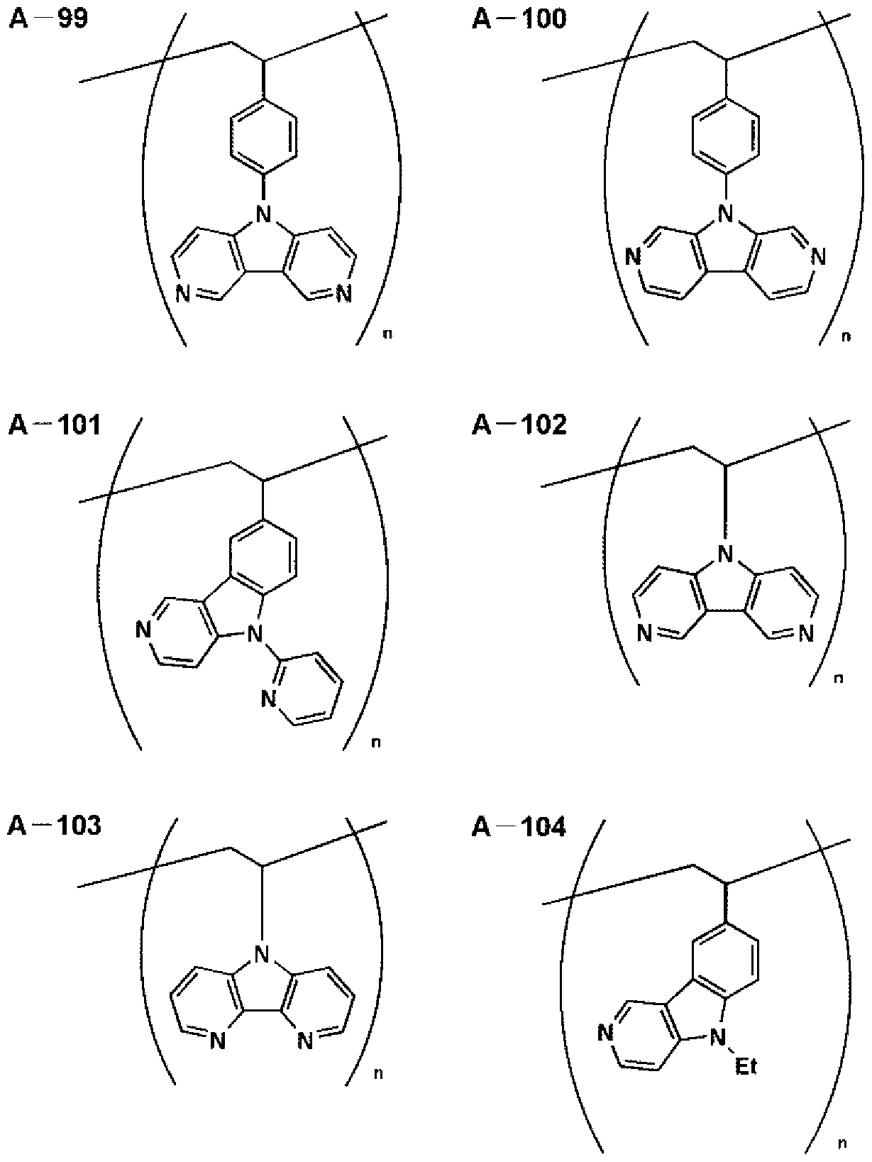
[0192] [化 58]
[0192] [Chemical 58]

[0193] [化 59]
[0193] [Chemical 59]

[0194] [化 60]
A— 121 [0194] [Chemical 60] A—121


[0196] [化 62]
 [0196] [Chemical 62]
7979
3874 3874

[0197] [化 6
[0197] [of 6

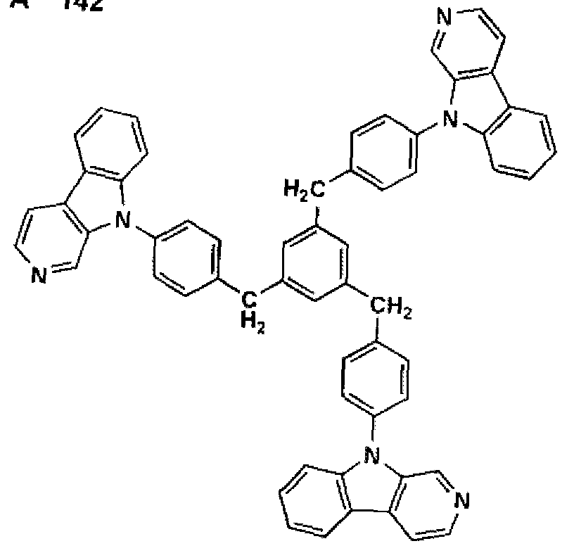
[0198] [化 64]
[0198] [Chemical 64]

[0199] [化 65]
[0199] [Chemical 65]
A— 147 A—147


[0201] [化 67]
[0201] [Chemical 67]
[89^ ] [2020] [89 ^] [2020]

^ひ 0£/900Zdf/ェ:) d ャ8 1^8£0I/900Z OAV
A— 158 A— 159 ^^ 0 £ / 900Zdf / e :) d8 8 ^^ 8 £ 0I / 900Z OAV A— 158 A— 159


[0204] [化 70] [0204] [Chemical 70]
A 170
 A 170
A 170
[0205] [化 71]
A一 171 A— 172 [0205] [Chemical 71] A one 171 A— 172

72]
72]


本発明に係る発光層は、上記化合物を、例えば、真空蒸着法、スピンコート法、キ ヤスト法、 LB法などの公知の薄膜ィ匕法により製膜して形成することができる。発光層 としての膜厚は特に制限はないが、通常は 5nm〜5 mの範囲で選ばれる。この発 光層はこれらの発光材料一種または二種以上力もなる一層構造であってもよ!/、し、あ るいは同一組成または異種組成の複数層からなる積層構造であってもよ!/ヽ。
[0208] また、この発光層は特開昭 57— 51781号公報に記載されているように、榭脂など の結着材と共に上記発光材料を溶剤に溶力して溶液とした後、これをスピンコート法 などにより薄膜ィ匕して形成することができる。このようにして形成された発光層の膜厚 については特に制限はなぐ状況に応じて適宜選択することができるが、通常は 5nm 〜5 μ mの範囲である。 The light emitting layer according to the present invention can be formed by forming the above compound by a known thin film method such as a vacuum deposition method, a spin coating method, a casting method, or an LB method. The thickness of the light emitting layer is not particularly limited, but is usually selected in the range of 5 nm to 5 m. This light emitting layer may be a single layer structure having one or more of these light emitting materials and / or a laminated structure composed of a plurality of layers having the same composition or different compositions! /ヽ. [0208] Further, as described in JP-A-57-51781, this light-emitting layer is made into a solution by dissolving the above-mentioned light-emitting material in a solvent together with a binder such as a resin. It can be formed as a thin film by spin coating or the like. The film thickness of the light-emitting layer thus formed can be appropriately selected according to the situation where there is no particular limitation, but is usually in the range of 5 nm to 5 μm.
[0209] 《阻止層:電子阻止層、正孔阻止層》 [0209] << Blocking layer: electron blocking layer, hole blocking layer >>
本発明に係る阻止層(例えば、電子阻止層、正孔阻止層)について説明する。本発 明に係る阻止層の膜厚としては好ましくは 3〜: LOOnmであり、更に好ましくは 5〜30 nmで teる o The blocking layer (for example, electron blocking layer, hole blocking layer) according to the present invention will be described. The thickness of the blocking layer according to the present invention is preferably 3 to: LOOnm, more preferably 5 to 30 nm.
[0210] (正孔阻止層) [0210] (Hole blocking layer)
正孔阻止層とは広い意味では電子輸送層の機能を有し、電子を輸送する機能を有 しつつ正孔を輸送する能力が著しく小さい材料力 なり、電子を輸送しつつ正孔を阻 止することで電子と正孔の再結合確率を向上させることができる。 In a broad sense, the hole blocking layer has the function of an electron transport layer, which is a material force that has the function of transporting electrons while transporting holes and is extremely small, and blocks holes while transporting electrons. By doing so, the probability of recombination of electrons and holes can be improved.
[0211] 本発明においては、発光層に隣接する隣接層、例えば、正孔阻止層、電子阻止層 等に、本発明の有機 EL素子用材料を正孔阻止層に好ましく用いることができる。 In the present invention, the organic EL device material of the present invention can be preferably used for the hole blocking layer in an adjacent layer adjacent to the light emitting layer, such as a hole blocking layer and an electron blocking layer.
[0212] 正孔阻止層としては、例えば、特開平 11 204258号公報、同 11 204359号公 報、及び「有機 EL素子とその工業化最前線(1998年 11月 30日 ェヌ'ティー 'エス 社発行)」の 237頁等に記載の正孔阻止(ホールブロック)層等を本発明に係る正孔 阻止層として適用可能である。また、後述する電子輸送層の構成を必要に応じて、本 発明に係る正孔阻止層として用いることができる。 [0212] Examples of the hole blocking layer include, for example, Japanese Patent Application Laid-Open Nos. 11 204258 and 11 204359, and “The Front Line of Organic EL Devices and Their Industrialization (November 30, 1998, NTT Corporation) The hole blocking (hole blocking) layer described in page 237 of “Issuance”) is applicable as the hole blocking layer according to the present invention. Moreover, the structure of the electron carrying layer mentioned later can be used as a hole-blocking layer concerning this invention as needed.
[0213] 本発明に係る正孔阻止層は、前記一般式(1)で表される化合物を含有することが 好ましい。また、本発明に係る正孔阻止層には、ボロン誘導体が含まれることが好ま しい。 [0213] The hole blocking layer according to the present invention preferably contains the compound represented by the general formula (1). The hole blocking layer according to the present invention preferably contains a boron derivative.
[0214] (電子阻止層) [0214] (Electron blocking layer)
一方、電子阻止層とは広い意味では正孔輸送層の機能を有し、正孔を輸送する機 能を有しつつ電子を輸送する能力が著しく小さい材料力 なり、正孔を輸送しつつ電 子を阻止することで電子と正孔の再結合確率を向上させることができる。また、後述 する正孔輸送層の構成を必要に応じて電子阻止層として用いることができる。
[0215] また、本発明においては、発光層に隣接する隣接層、即ち正孔阻止層、電子阻止 層に、上記の本発明の有機 EL素子用材料を用いることが好ましぐ特に正孔阻止層 に用いることが好ましい。 On the other hand, the electron blocking layer has the function of a hole transport layer in a broad sense, and is a material force that has a function of transporting holes and an extremely small capacity of transporting electrons, and transports holes while transporting holes. The probability of recombination of electrons and holes can be improved by blocking the children. Moreover, the structure of the positive hole transport layer mentioned later can be used as an electron blocking layer as needed. [0215] In the present invention, it is preferable to use the organic EL device material of the present invention described above for the adjacent layer adjacent to the light-emitting layer, that is, the hole blocking layer and the electron blocking layer. It is preferable to use it for the layer.
[0216] 《正孔輸送層》 [0216] 《Hole transport layer》
正孔輸送層とは正孔を輸送する機能を有する材料を含み、広い意味で正孔注入 層、電子阻止層も正孔輸送層に含まれる。正孔輸送層は単層もしくは複数層設ける ことができる。 The hole transport layer includes a material having a function of transporting holes, and in a broad sense, a hole injection layer and an electron blocking layer are also included in the hole transport layer. The hole transport layer can be provided as a single layer or a plurality of layers.
[0217] 正孔輸送材料としては特に制限はなぐ従来、光導伝材料において、正孔の電荷 注入輸送材料として慣用されて 、るものや EL素子の正孔注入層、正孔輸送層に使 用される公知のものの中から任意のものを選択して用いることができる。 [0217] As a hole transport material, there is no particular limitation. Conventionally, in a photoconductive material, it is commonly used as a hole charge injection transport material, and used for a hole injection layer and a hole transport layer of an EL element. Any known one can be selected and used.
[0218] 正孔輸送材料は正孔の注入もしくは輸送、電子の障壁性の!/、ずれかを有するもの であり、有機物、無機物のいずれであってもよい。例えば、トリァゾール誘導体、ォキ サジァゾール誘導体、イミダゾール誘導体、ポリアリールアルカン誘導体、ピラゾリン 誘導体及びピラゾロン誘導体、フ 二レンジァミン誘導体、ァリールァミン誘導体、アミ ノ置換カルコン誘導体、ォキサゾール誘導体、スチリルアントラセン誘導体、フルォレ ノン誘導体、ヒドラゾン誘導体、スチルベン誘導体、シラザン誘導体、ァニリン系共重 合体、また、導電性高分子オリゴマー、特にチォフェンオリゴマー等が挙げられる。 [0218] The hole transport material has a hole injection or transport, electron barrier property! /, Or a deviation, and may be either organic or inorganic. For example, triazole derivatives, oxadiazole derivatives, imidazole derivatives, polyarylalkane derivatives, pyrazoline derivatives and pyrazolone derivatives, phenylenediamine derivatives, arylamine derivatives, amino-substituted chalcone derivatives, oxazole derivatives, styrylanthracene derivatives, fluorenone derivatives, hydrazones Derivatives, stilbene derivatives, silazane derivatives, aniline copolymers, and conductive polymer oligomers, particularly thiophene oligomers.
[0219] 正孔輸送材料としては上記のものを使用することができる力 ボルフイリンィ匕合物、 芳香族第三級ァミン化合物及びスチリルアミン化合物、特に芳香族第三級アミンィ匕 合物を用いることが好まし 、。 [0219] The ability to use the above-mentioned materials as the hole transporting material. Volphilin compounds, aromatic tertiary amine compounds and styryl amine compounds, especially aromatic tertiary amine compounds may be used. I like it.
[0220] 芳香族第三級アミンィ匕合物及びスチリルアミンィ匕合物の代表例としては、 N, N, N ' , N' —テトラフエ-ル一 4, 4' —ジァミノフエ-ル; N, N' —ジフエ-ル一 N, N, —ビス(3—メチルフエ-ル)一〔1, 1' —ビフエ-ル〕一 4, 4' —ジァミン(TPD) ; 2, 2 -ビス(4 ジ— p トリルァミノフエ-ル)プロパン; 1 , 1 ビス(4 ジ— p トリルァ ミノフエ-ル)シクロへキサン; N, N, N' , N' —テトラ一 p トリル一 4, 4' —ジアミ ノビフエ-ル; 1 , 1 ビス(4 ジ一 p トリルァミノフエ-ル) 4 フエ-ルシクロへキ サン;ビス(4 -ジメチルァミノ 2 メチルフエ-ル)フエニルメタン;ビス(4 ジ一 p— トリルァミノフエ-ル)フエ-ルメタン; N, N' —ジフエ-ルー N, N' —ジ(4—メトキシ
フエ-ル) 4, 4' —ジアミノビフエ-ル; N, N, N' , N' —テトラフエ-ルー 4, 4 ' ージアミノジフエ-ルエーテル; 4, 4 '—ビス(ジフエ-ルァミノ)クオードリフエ-ル; N, N, N トリ(p トリル)ァミン; 4— (ジ— p トリルァミノ)— 4' —〔4— (ジ— p ト リルァミノ)スチリル〕スチルベン; 4— N, N ジフエ-ルァミノ—(2 ジフエ-ルビ- ノレ)ベンゼン; 3—メトキシー^ —N, N ジフエニノレアミノスチノレベンゼン; N—フエ 二ルカルバゾール、更には米国特許第 5, 061, 569号明細書に記載されている 2個 の縮合芳香族環を分子内に有するもの、例えば、 4, 4' ビス〔N—(1 ナフチル) —N—フエ-ルァミノ〕ビフエ-ル(NPD)、特開平 4— 308688号公報に記載されて いるトリフエ-ルァミンユニットが 3つスターバースト型に連結された 4, ' , A" —トリ ス〔?^— (3—メチルフエ-ル)—N—フエ-ルァミノ〕トリフエ-ルァミン(MTDATA)等 が挙げられる。 [0220] Representative examples of aromatic tertiary amine compounds and styrylamine compounds include N, N, N ', N' —tetraphenyl 4, 4 '— diaminophenol; N, N '—Diphenyl 1 N, N, —Bis (3-methylphenol) 1 [1, 1' —Biphenyl] 4,4 ′ —Diamine (TPD); 2, 2-bis (4 di — P-tolylaminophenol) propane; 1, 1 bis (4 di-p-tolylaminophenol) cyclohexane; N, N, N ′, N ′ —tetra-p-tolyl-1,4,4′—diaminobiphenol 1, 1 bis (4 di-l-triaminophenol) 4-phenylcyclohexane; bis (4-dimethylamino-2-methylphenol) phenyl methane; bis (4 di-l-triaminophenol) phenol methane; N , N '—Dihue-Lu N, N' —Di (4-methoxy 4,4'-diaminobiphenyl; N, N, N ', N'-tetraphenyl 4,4'-diaminodiether ether; 4,4'-bis (diphenylamino) quadule; N , N, N Tri (p-tolyl) amine; 4— (Di-p-tolylamino) —4 ′ — [4 -— (Di-p-tolylamino) styryl] stilbene; 4-—N, N diphenylamino- (2 diphenyl) Ruby-Nole) benzene; 3-methoxy-^-N, N diphenylenosamino benzene; N-phenylcarbazole, and also two of those described in US Pat. No. 5,061,569. Having a condensed aromatic ring in the molecule, for example, as described in 4,4′bis [N- (1 naphthyl) -N-phenylamino] biphenyl (NPD), JP-A-4-308688 Three triphenylamine units connected in a starburst type 4, ', A "—Tris [? ^ — (3 Mechirufue - Le) -N- Hue - Ruamino] bird whistle - Ruamin (MTDATA) and the like.
[0221] 更にこれらの材料を高分子鎖に導入した、またはこれらの材料を高分子の主鎖とし た高分子材料を用いることもできる。また、 P型— Si、 p型— SiC等の無機化合物も正 孔注入材料、正孔輸送材料として使用することができる。また、本発明においては、 正孔輸送層の正孔輸送材料は 415nm以下に蛍光極大波長を有することが好ましく 、リン光の 0— 0バンドが 450nm以下であることが更に好ましい。また、正孔輸送材料 は高 Tgであることが好まし!/、。 [0221] Further, a polymer material in which these materials are introduced into a polymer chain or these materials as a polymer main chain can also be used. Inorganic compounds such as P-type-Si and p-type-SiC can also be used as the hole injection material and hole transport material. In the present invention, the hole transport material of the hole transport layer preferably has a fluorescence maximum wavelength at 415 nm or less, and more preferably has a 0-0 band of phosphorescence of 450 nm or less. Also, the hole transport material is preferably high Tg! /.
[0222] この正孔輸送層は、上記正孔輸送材料を、例えば、真空蒸着法、スピンコート法、 キャスト法、インクジェット法、 LB法等の公知の方法により、薄膜化することにより形成 することができる。正孔輸送層の膜厚については特に制限はないが、通常は 5〜500 Onm程度である。この正孔輸送層は上記材料の一種または二種以上からなる一層 構造であってもよい。 [0222] This hole transport layer is formed by thinning the hole transport material by a known method such as a vacuum deposition method, a spin coating method, a casting method, an ink jet method, or an LB method. Can do. The film thickness of the hole transport layer is not particularly limited, but is usually about 5 to 500 Onm. The hole transport layer may have a single layer structure composed of one or more of the above materials.
[0223] 《電子輸送層》 [0223] 《Electron Transport Layer》
電子輸送層とは電子を輸送する機能を有する材料力 なり、広い意味で電子注入 層、正孔阻止層も電子輸送層に含まれる。電子輸送層は単層もしくは複数層を設け ることがでさる。 The electron transport layer is a material force having a function of transporting electrons, and in a broad sense, an electron injection layer and a hole blocking layer are also included in the electron transport layer. The electron transport layer can be a single layer or a plurality of layers.
[0224] 従来、単層の電子輸送層、及び複数層とする場合は発光層に対して陰極側に隣 接する電子輸送層に用いられる電子輸送材料 (正孔阻止材料を兼ねる)としては、下
記の材料が知られている。更に、電子輸送層は陰極より注入された電子を発光層に 伝達する機能を有していればよぐその材料としては従来公知の化合物の中から任 意のものを選択して用いることができる。 [0224] Conventionally, when a single electron transport layer and a plurality of layers are used, an electron transport material (also serving as a hole blocking material) used for an electron transport layer adjacent to the light emitting layer on the cathode side is as follows. The following materials are known. Furthermore, the electron transport layer only needs to have a function of transmitting electrons injected from the cathode to the light emitting layer, and any material can be selected from conventionally known compounds. .
[0225] この電子輸送層に用いられる材料 (以下、電子輸送材料という)の例としては、 -ト 口置換フルオレン誘導体、ジフヱ-ルキノン誘導体、チォピランジオキシド誘導体、ナ フタレンペリレンなどの複素環テトラカルボン酸無水物、カルボジイミド、フレオレニリ デンメタン誘導体、アントラキノジメタン及びアントロン誘導体、ォキサジァゾール誘導 体などが挙げられる。更に上記ォキサジァゾール誘導体において、ォキサジァゾ一 ル環の酸素原子を硫黄原子に置換したチアジアゾール誘導体、電子吸引基として知 られて!ヽるキノキサリン環を有するキノキサリン誘導体も、電子輸送材料として用いる ことができる。 [0225] Examples of materials used for this electron transport layer (hereinafter referred to as electron transport materials) include: -to-substituted fluorene derivatives, diphenylquinone derivatives, thiopyran dioxide derivatives, and heterocyclic rings such as naphthalene perylene. Examples thereof include tetracarboxylic anhydrides, carbodiimides, fluorenylidenemethane derivatives, anthraquinodimethane and anthrone derivatives, and oxadiazole derivatives. Furthermore, in the above oxadiazole derivative, a thiadiazole derivative in which the oxygen atom of the oxadiazole ring is substituted with a sulfur atom, or a quinoxaline derivative having a quinoxaline ring known as an electron withdrawing group can also be used as an electron transport material.
[0226] 更にこれらの材料を高分子鎖に導入した、またはこれらの材料を高分子の主鎖とし た高分子材料を用いることもできる。 [0226] Further, a polymer material in which these materials are introduced into a polymer chain or these materials as a polymer main chain can also be used.
[0227] また、 8 キノリノール誘導体の金属錯体、例えば、トリス(8 キノリノール)アルミ- ゥム(Alq)、トリス(5, 7—ジクロロ一 8—キノリノール)アルミニウム、トリス(5, 7—ジブ ロモ一 8 キノリノール)アルミニウム、トリス(2 メチル 8 -キノリノール)アルミ-ゥ ム、トリス(5—メチル 8—キノリノール)アルミニウム、ビス(8—キノリノール)亜鉛(Zn q)など、及びこれらの金属錯体の中心金属が In、 Mg、 Cu、 Ca、 Sn、 Gaまたは Pbに 置き替わった金属錯体も電子輸送材料として用いることができる。その他、メタルフリ 一もしくはメタルフタロシアニン、またはそれらの末端がアルキル基ゃスルホン酸基な どで置換されているものも、電子輸送材料として好ましく用いることができる。また、発 光層の材料として例示したジスチリルビラジン誘導体も、電子輸送材料として用いる ことができるし、正孔注入層、正孔輸送層と同様に、 n型— Si、 n型— SiCなどの無機 半導体も電子輸送材料として用いることができる。 [0227] In addition, metal complexes of 8 quinolinol derivatives, such as tris (8 quinolinol) aluminum (Alq), tris (5,7-dichloro-1-8-quinolinol) aluminum, tris (5,7-dibromo 1 8 quinolinol) aluminum, tris (2methyl 8-quinolinol) aluminum, tris (5-methyl 8-quinolinol) aluminum, bis (8-quinolinol) zinc (Zn q), and the central metals of these metal complexes Metal complexes in which In, Mg, Cu, Ca, Sn, Ga, or Pb are replaced can also be used as electron transport materials. In addition, metal free or metal phthalocyanine, or those having terminal ends substituted with an alkyl group or a sulfonic acid group can be preferably used as the electron transporting material. In addition, the distyrylvirazine derivative exemplified as the material for the light emitting layer can also be used as an electron transport material, and, like the hole injection layer and the hole transport layer, n-type-Si, n-type-SiC, etc. These inorganic semiconductors can also be used as electron transport materials.
[0228] この電子輸送層は上記電子輸送材料を、例えば、真空蒸着法、スピンコート法、キ ヤスト法、インクジェット法、 LB法等の公知の方法により、薄膜化することにより形成す ることができる。電子輸送層の膜厚については特に制限はないが、通常は 5〜5000 nm程度である。この電子輸送層は上記材料の一種または二種以上からなる一層構
造であってもよい。 [0228] The electron transport layer may be formed by thinning the electron transport material by a known method such as a vacuum deposition method, a spin coating method, a casting method, an ink jet method, or an LB method. it can. Although there is no restriction | limiting in particular about the film thickness of an electron carrying layer, Usually, it is about 5-5000 nm. This electron transport layer has a single layer structure composed of one or more of the above materials. It may be made.
[0229] 次に、本発明の有機 EL素子の構成層として用いられる、注入層について説明する Next, an injection layer used as a constituent layer of the organic EL element of the present invention will be described.
[0230] 《注入層:電子注入層、正孔注入層》 [0230] <Injection layer: electron injection layer, hole injection layer>
注入層は必要に応じて設け、電子注入層と正孔注入層があり、上記のごとく陽極と 発光層または正孔輸送層の間、及び陰極と発光層または電子輸送層との間に存在 させてちょい。 The injection layer is provided as necessary, and has an electron injection layer and a hole injection layer, and as described above, exists between the anode and the light emitting layer or hole transport layer and between the cathode and the light emitting layer or electron transport layer. Hey.
[0231] 注入層とは、駆動電圧低下や発光輝度向上のために電極と有機層間に設けられる 層のことで、「有機 EL素子とその工業ィ匕最前線(1998年 11月 30日 ェヌ'ティー'ェ ス社発行)」の第 2編第 2章「電極材料」(123〜166頁)に詳細に記載されており、正 孔注入層(陽極バッファ一層)と電子注入層(陰極バッファ一層)とがある。 [0231] The injection layer is a layer provided between the electrode and the organic layer in order to reduce the drive voltage and improve the luminance of the light emission. “The organic EL element and its industry front line (November 30, 1998) Chapter 2 “Electrode materials” (pages 123-166) of “Part 2” of “Tees Co., Ltd.”) describes the details of the hole injection layer (anode buffer layer) and the electron injection layer (cathode buffer). One layer).
[0232] 陽極バッファ一層(正孔注入層)は、特開平 9— 45479号公報、同 9 260062号 公報、同 8— 288069号公報等にもその詳細が記載されており、具体例として、銅フ タロシアニンに代表されるフタロシアニンバッファ一層、酸ィ匕バナジウムに代表される 酸化物バッファ一層、アモルファスカーボンバッファ一層、ポリア-リン(ェメラルディ ン)やポリチォフェン等の導電性高分子を用いた高分子バッファ一層等が挙げられる [0232] The details of the anode buffer layer (hole injection layer) are also described in JP-A-9-45479, JP-A-9260062, JP-A-8-288069 and the like. A phthalocyanine buffer layer typified by phthalocyanine, an oxide buffer layer typified by vanadium oxide, an amorphous carbon buffer layer, a polymer buffer layer using a conductive polymer such as polyarene (emeraldine) or polythiophene Etc.
[0233] 陰極バッファ一層(電子注入層)は、特開平 6— 325871号公報、同 9 17574号 公報、同 10— 74586号公報等にもその詳細が記載されており、具体的にはストロン チウムゃアルミニウム等に代表される金属バッファ一層、フッ化リチウムに代表される アルカリ金属化合物バッファ一層、フッ化マグネシウムに代表されるアルカリ土類金 属化合物バッファ一層、酸ィヒアルミニウムに代表される酸ィヒ物バッファ一層等が挙げ られる。 [0233] Details of the cathode buffer layer (electron injection layer) are also described in JP-A-6-325871, JP-A-9-17574, JP-A-10-74586, and the like. Specifically, strontium Metal buffer layer typified by aluminum, etc., alkali metal compound buffer layer typified by lithium fluoride, alkaline earth metal compound buffer layer typified by magnesium fluoride, acid salt typified by acid aluminum One thing buffer is one example.
[0234] 上記バッファ一層(注入層)はごく薄い膜であることが望ましぐ素材にもよるがその 膜厚は 0. 1〜: LOOnmの範囲が好ましい。 [0234] The buffer layer (injection layer) preferably has a very thin film thickness, although the film thickness is preferably in the range of 0.1 to LOOnm.
[0235] この注入層は上記材料を、例えば、真空蒸着法、スピンコート法、キャスト法、インク ジェット法、 LB法等の公知の方法により、薄膜ィ匕することにより形成することができる 。注入層の膜厚については特に制限はないが、通常は 5〜5000nm程度である。こ
の注入層は上記材料の一種または二種以上力もなる一層構造であってもよい。 [0235] This injection layer can be formed by thin-filming the above material by a known method such as a vacuum deposition method, a spin coating method, a casting method, an ink jet method, or an LB method. The thickness of the injection layer is not particularly limited, but is usually about 5 to 5000 nm. This The injection layer may have a single-layer structure that also has one or more of the above materials.
[0236] 《陽極》 [0236] 《Anode》
本発明の有機 EL素子に係る陽極としては、仕事関数の大きい (4eV以上)金属、 合金、電気伝導性化合物及びこれらの混合物を電極物質とするものが好ましく用い られる。このような電極物質の具体例としては、 Au等の金属、 Cul、インジウムチンォ キシド (ITO)、 SnO、 ZnO等の導電性透明材料が挙げられる。また、 IDIXO (In O As the anode of the organic EL device of the present invention, an electrode material made of a metal, an alloy, an electrically conductive compound or a mixture thereof having a high work function (4 eV or more) is preferably used. Specific examples of such electrode substances include conductive transparent materials such as metals such as Au, Cul, indium tin oxide (ITO), SnO, and ZnO. IDIXO (In O
2 2 3 2 2 3
-ZnO)等非晶質で透明導電膜を作製可能な材料を用いてもよ!ヽ。陽極はこれらの 電極物質を蒸着やスパッタリング等の方法により薄膜を形成させ、フォトリソグラフィー 法で所望の形状のパターンを形成してもよぐあるいはパターン精度をあまり必要とし ない場合は(100 m以上程度)、上記電極物質の蒸着やスパッタリング時に所望の 形状のマスクを介してパターンを形成してもよい。この陽極より発光を取り出す場合に は、透過率を 10%より大きくすることが望ましぐまた、陽極としてのシート抵抗は数百 ΩΖ口以下が好ましい。更に膜厚は材料にもよる力 通常 10〜: L000nm、好ましく は 10〜200nmの範囲で選ばれる。 -ZnO) or other amorphous material that can produce a transparent conductive film may be used. For the anode, these electrode materials can be formed into a thin film by vapor deposition or sputtering, and a pattern of the desired shape can be formed by photolithography, or when pattern accuracy is not so high (about 100 m or more) ), A pattern may be formed through a mask having a desired shape when the electrode material is deposited or sputtered. When light emission is taken out from this anode, it is desirable to have a transmittance of more than 10%, and the sheet resistance as the anode is preferably several hundreds Ω or less. Further, the film thickness is a force depending on the material. Usually, 10 to L000 nm, preferably 10 to 200 nm is selected.
[0237] 《陰極》 [0237] 《Cathode》
一方、本発明に係る陰極としては、仕事関数の小さい (4eV以下)金属 (電子注入 性金属と称する)、合金、電気伝導性化合物及びこれらの混合物を電極物質とするも のが用いられる。このような電極物質の具体例としては、ナトリウム、ナトリウム一力リウ ム合金、マグネシウム、リチウム、マグネシウム Z銅混合物、マグネシウム Z銀混合物 、マグネシウム /アルミニウム混合物、マグネシウム Zインジウム混合物、アルミニウム Z酸ィ匕アルミニウム (Al O )混合物、インジウム、リチウム Zアルミニウム混合物、希 On the other hand, as the cathode according to the present invention, a material having a low work function (4 eV or less) metal (referred to as an electron injecting metal), an alloy, an electrically conductive compound, and a mixture thereof is used. Specific examples of such electrode materials include sodium, sodium-powered rhodium alloy, magnesium, lithium, magnesium Z copper mixture, magnesium Z silver mixture, magnesium / aluminum mixture, magnesium Z indium mixture, aluminum Z acid aluminum (Al 2 O 3) mixture, indium, lithium Z aluminum mixture, dilute
2 3 twenty three
土類金属等が挙げられる。これらの中で、電子注入性及び酸化等に対する耐久性の 点から、電子注入性金属とこれより仕事関数の値が大きく安定な金属である第二金 属との混合物、例えば、マグネシウム Z銀混合物、マグネシウム Zアルミニウム混合 物、マグネシウム Zインジウム混合物、アルミニウム Z酸ィ匕アルミニウム (Al O )混合 Examples include earth metals. Among these, from the viewpoint of electron injectability and durability against oxidation, etc., a mixture of an electron injecting metal and a second metal which is a stable metal having a larger work function value than this, for example, a magnesium Z silver mixture , Magnesium Z Aluminum Mixture, Magnesium Z Indium Mixture, Aluminum Z Acid-Aluminum (Al O) Mixture
2 3 物、リチウム Zアルミニウム混合物、アルミニウム等が好適である。陰極はこれらの電 極物質を蒸着やスパッタリング等の方法により、薄膜を形成させることにより作製する ことができる。また、陰極としてのシート抵抗は数百 Ω /口以下が好ましぐ膜厚は通
常 10〜: L000nm、好ましくは 50〜200nmの範囲で選ばれる。なお、発光を透過さ せるため、有機 EL素子の陽極または陰極のいずれか一方が、透明または半透明で あれば発光輝度が向上し好都合である。 2 3, lithium Z aluminum mixture, aluminum and the like are suitable. The cathode can be produced by forming a thin film of these electrode materials by a method such as vapor deposition or sputtering. In addition, the sheet resistance as a cathode is several hundred Ω / mouth or less, and the preferred film thickness is Usually 10 to: L000 nm, preferably 50 to 200 nm. In order to transmit light emission, it is convenient that either the anode or the cathode of the organic EL element is transparent or translucent to improve the light emission luminance.
[0238] 《基体 (基板、基材、支持体等とも!ヽぅ)》 [0238] <Substrate (both substrate, substrate, support, etc.!)>
本発明の有機 EL素子に係る基体としては、ガラス、プラスチック等の種類には特に 限定はなぐまた透明のものであれば特に制限はないが、好ましく用いられる基板と しては、例えば、ガラス、石英、光透過性榭脂フィルムを挙げることができる。特に好 ま 、基体は、有機 EL素子にフレキシブル性を与えることが可能な榭脂フィルムであ る。 The substrate of the organic EL device of the present invention is not particularly limited as long as it is transparent or transparent, and there are no particular restrictions on the type of glass, plastic, etc. Examples of substrates that are preferably used include glass, Examples thereof include quartz and a light-transmitting resin film. Particularly preferably, the substrate is a resin film capable of giving flexibility to the organic EL element.
[0239] 榭脂フィルムとしては、例えば、ポリエチレンテレフタレート(PET)、ポリエチレンナ フタレート(PEN)、ポリエーテルスルホン(PES)、ポリエーテルイミド、ポリエーテル エーテルケトン、ポリフエ-レンスルフイド、ポリアリレート、ポリイミド、ポリカーボネート (PC)、セルローストリアセテート (TAC)、セルロースアセテートプロピオネート(CAP )等力 なるフィルム等が挙げられる。 [0239] Examples of the resin film include polyethylene terephthalate (PET), polyethylene naphthalate (PEN), polyethersulfone (PES), polyetherimide, polyetheretherketone, polyphenylene sulfide, polyarylate, polyimide, and polycarbonate. (PC), cellulose triacetate (TAC), cellulose acetate propionate (CAP) and the like.
[0240] 榭脂フィルムの表面には、無機物もしくは有機物の被膜またはその両者のハイプリ ッド被膜が形成されていてもよぐ水蒸気透過率が 0. 01gZm2'dayatm以下の高 ノ リア性フィルムであることが好まし ヽ。 [0240] On the surface of the resin film, an inorganic film or an organic film, or a hybrid film of both of them may be formed, and the water vapor transmission rate is 0.01 gZm 2 'dayatm or less. I prefer to be there.
[0241] 本発明の有機 EL素子において、発光の室温における外部取り出し量子効率は、 1 %以上であることが好ましぐより好ましくは 2%以上である。ここに、外部取り出し量 子効率 (%) =有機 EL素子外部に発光した光子数 Z有機 EL素子に流した電子数 X 100である。 [0241] In the organic EL device of the present invention, the external extraction quantum efficiency of light emission at room temperature is preferably 1% or more, more preferably 2% or more. Here, the external extraction quantum efficiency (%) = the number of photons emitted outside the organic EL element Z = the number of electrons flown through the organic EL element × 100.
[0242] また、カラーフィルタ一等の色相改良フィルタ一等を併用してもよい。 [0242] Further, a hue improving filter such as a color filter may be used in combination.
[0243] 照明用途で用いる場合には、発光ムラを低減させるために粗面加工したフィルム( アンチグレアフィルム等)を併用することもできる。 [0243] When used for illumination, a roughened film (such as an antiglare film) can be used in combination in order to reduce unevenness in light emission.
[0244] 多色表示装置として用いる場合は少なくとも 2種類の異なる発光極大波長を有する 有機 EL素子カゝらなるが、有機 EL素子を作製する好適な例を説明する。 [0244] When used as a multicolor display device, the organic EL element having at least two different emission maximum wavelengths will be described. A preferred example of producing an organic EL element will be described.
[0245] 《有機 EL素子の作製方法》 [0245] <Method for manufacturing organic EL element>
本発明の有機 EL素子の作製方法の一例として、陽極/正孔注入層/正孔輸送層
Z発光層 Z正孔阻止層 Z電子輸送層 Z陰極バッファ一層 Z陰極からなる有機 EL 素子の作製法について説明する。 As an example of a method for producing the organic EL device of the present invention, an anode / hole injection layer / hole transport layer Z light-emitting layer Z hole blocking layer Z electron transport layer Z cathode buffer layer An organic EL device comprising a Z cathode will be described.
[0246] まず適当な基体上に所望の電極物質、例えば、陽極用物質力 なる薄膜を 1 μ m 以下、好ましくは ΙΟηπ!〜 200nmの膜厚になるように、蒸着やスパッタリング等の方 法により形成させ、陽極を作製する。次に、この上に素子材料である正孔注入層、正 孔輸送層、発光層、正孔阻止層、電子輸送層等の有機化合物を含有する薄膜を形 成させる。 [0246] First, a desired electrode material, for example, a thin film having a material force for an anode is formed on a suitable substrate at 1 μm or less, preferably ΙΟηπ! An anode is formed by a method such as vapor deposition or sputtering so as to have a film thickness of ˜200 nm. Next, a thin film containing an organic compound such as a hole injection layer, a hole transport layer, a light emitting layer, a hole blocking layer, and an electron transport layer, which is an element material, is formed thereon.
[0247] この有機化合物を含有する薄膜の薄膜ィ匕の方法としては、前記の如くスピンコート 法、キャスト法、インクジェット法、蒸着法、印刷法等があるが、均質な膜が得られや すぐ且つピンホールが生成しにくい等の点から、真空蒸着法またはスピンコート法 が特に好ましい。更に層ごとに異なる製膜法を適用してもよい。製膜に蒸着法を採用 する場合、その蒸着条件は、使用する化合物の種類等により異なるが、一般にボート 加熱温度 50〜450°C、真空度 10— 6〜: LO— 2Pa、蒸着速度 0. 01〜50nmZ秒、基板 温度— 50〜300°C、膜厚 0. lnm〜5 μ mの範囲で適宜選ぶことが望ましい。 [0247] As described above, there are spin coating method, casting method, ink jet method, vapor deposition method, printing method and the like as a method for forming a thin film containing an organic compound, but it is easy to obtain a homogeneous film. In view of the difficulty of generating pinholes, vacuum deposition or spin coating is particularly preferable. Further, a different film forming method may be applied for each layer. When employing the vapor deposition film, the deposition conditions may vary due to kinds of materials used, generally boat temperature 50 to 450 ° C, vacuum degree of 10- 6 ~: LO- 2 Pa, deposition rate 0 It is desirable to select as appropriate within the range of 01 to 50 nmZ seconds, substrate temperature—50 to 300 ° C., and film thickness of 0.1 nm to 5 μm.
[0248] これらの層の形成後、その上に陰極用物質力もなる薄膜を、 1 μ m以下好ましくは 5 0nm〜200nmの範囲の膜厚になるように、例えば、蒸着やスパッタリング等の方法 により形成させ、陰極を設けることにより所望の有機 EL素子が得られる。この有機 EL 素子の作製は、一回の真空引きで一貫して正孔注入層から陰極まで作製するのが 好ましいが、途中で取り出して異なる製膜法を施しても構わない。その際、作業を乾 燥不活性ガス雰囲気下で行う等の配慮が必要となる。 [0248] After the formation of these layers, a thin film having a cathode material force is formed thereon by 1 μm or less, preferably by a method such as vapor deposition or sputtering so as to have a film thickness in the range of 50 nm to 200 nm. By forming the cathode and providing the cathode, a desired organic EL device can be obtained. The organic EL device is preferably manufactured from the hole injection layer to the cathode consistently by a single evacuation, but it may be taken out halfway and subjected to different film forming methods. At that time, it is necessary to consider that the work is performed in a dry inert gas atmosphere.
[0249] 《表示装置》 [0249] <Display device>
本発明の表示装置について説明する。 The display device of the present invention will be described.
[0250] 本発明の表示装置は単色でも多色でもよいが、ここでは多色表示装置について説 明する。多色表示装置の場合は発光層形成時のみシャドーマスクを設け、一面に蒸 着法、キャスト法、スピンコート法、インクジェット法、印刷法等で膜を形成できる。 [0250] Although the display device of the present invention may be monochromatic or multicolored, a multicolor display device will be described here. In the case of a multicolor display device, a shadow mask is provided only at the time of forming a light emitting layer, and a film can be formed on one surface by a vapor deposition method, a casting method, a spin coating method, an ink jet method, a printing method, or the like.
[0251] 発光層のみパターニングを行う場合その方法に限定はないが、好ましくは蒸着法、 インクジェット法、印刷法である。蒸着法を用いる場合においては、シャドーマスクを 用いたパター-ングが好ましい。また作製順序を逆にして、陰極、電子輸送層、正孔
阻止層、発光層、正孔輸送層、陽極の順に作製することも可能である。 [0251] In the case of patterning only the light emitting layer, the method is not limited, but the vapor deposition method, the inkjet method, and the printing method are preferable. In the case of using the vapor deposition method, patterning using a shadow mask is preferable. In addition, the production order is reversed, the cathode, the electron transport layer, the holes It is also possible to produce a blocking layer, a light emitting layer, a hole transport layer, and an anode in this order.
[0252] このようにして得られた多色表示装置に直流電圧を印加する場合には、陽極を +、 陰極を—の極性として電圧 2〜40V程度を印加すると発光が観測できる。また、逆の 極性で電圧を印加しても電流は流れずに発光は全く生じな!/ヽ。更に交流電圧を印加 する場合には、陽極が +、陰極が—の状態になったときのみ発光する。なお、印加 する交流の波形は任意でょ 、。 [0252] When a DC voltage is applied to the multicolor display device thus obtained, light emission can be observed by applying a voltage of about 2 to 40 V with the positive polarity of the anode and the negative polarity of the cathode. In addition, no current flows even when a voltage is applied with the opposite polarity, and no light emission occurs! / ヽ. In addition, when an AC voltage is applied, light is emitted only when the anode is in the + state and the cathode is in the-state. The AC waveform to be applied is arbitrary.
[0253] 多色表示装置は表示デバイス、ディスプレイ、各種発光光源として用いることができ る。表示デバイス、ディスプレイにおいて、青、赤、緑発光の 3種の有機 EL素子を用 いることにより、フルカラーの表示が可能となる。 [0253] The multicolor display device can be used as a display device, a display, and various light sources. Display devices and displays can be displayed in full color by using three types of organic EL elements that emit blue, red, and green light.
[0254] 表示デバイス、ディスプレイとしてはテレビ、ノ ソコン、モパイル機器、 AV機器、文 字放送表示、自動車内の情報表示等が挙げられる。特に静止画像や動画像を再生 する表示装置として使用してもよぐ動画再生用の表示装置として使用する場合の駆 動方式は単純マトリックス (パッシブマトリックス)方式でもアクティブマトリックス方式で もどちらでもよい。 [0254] Examples of the display device and display include a television, a computer, a mopile device, an AV device, a character broadcast display, and an information display in a car. In particular, the driving method when used as a display device for reproducing moving images, which may be used as a display device for reproducing still images or moving images, may be either a simple matrix (passive matrix) method or an active matrix method.
[0255] 発光光源としては家庭用照明、車内照明、時計や液晶用のバックライト、看板広告 、信号機、光記憶媒体の光源、電子写真複写機の光源、光通信処理機の光源、光 センサーの光源等が挙げられるがこれに限定するものではない。 [0255] Light emitting light sources include home lighting, interior lighting, clock and liquid crystal backlights, billboard advertisements, traffic lights, light sources for optical storage media, light sources for electrophotographic copying machines, light sources for optical communication processors, light sensors Although a light source etc. are mentioned, it is not limited to this.
[0256] 《照明装置》 [0256] 《Lighting device》
本発明の照明装置について説明する。 The lighting device of the present invention will be described.
[0257] 本発明の有機 EL素子に共振器構造を持たせた有機 EL素子として用いてもよぐこ のような共振器構造を有した有機 EL素子の使用目的としては、光記憶媒体の光源、 電子写真複写機の光源、光通信処理機の光源、光センサーの光源等が挙げられる 力 これらに限定されない。またレーザー発振をさせることにより、上記用途に使用し てもよい。 [0257] The organic EL element having a resonator structure as described above may be used as an organic EL element having a resonator structure in the organic EL element of the present invention. Examples include, but are not limited to, light sources for electrophotographic copying machines, light sources for optical communication processors, and light sources for optical sensors. Further, it may be used for the above application by causing laser oscillation.
[0258] また、本発明の有機 EL素子は、照明用や露光光源のような一種のランプとして使 用してもよいし、画像を投影するタイプのプロジェクシヨン装置や、静止画像や動画像 を直接視認するタイプの表示装置 (ディスプレイ)として使用してもよい。動画再生用 の表示装置として使用する場合の駆動方式は単純マトリックス (パッシブマトリックス)
方式でもアクティブマトリックス方式でもどちらでもよ 、。または異なる発光色を有する 本発明の有機 EL素子を 2種以上使用することにより、フルカラー表示装置を作製す ることが可能である。 [0258] Further, the organic EL device of the present invention may be used as a kind of lamp such as an illumination or exposure light source, a projection device of a type for projecting an image, a still image or a moving image. It may be used as a type of display device (display) that is directly visible. The drive system when used as a display device for video playback is a simple matrix (passive matrix) Either the method or the active matrix method. Alternatively, a full color display device can be produced by using two or more organic EL elements of the present invention having different emission colors.
[0259] 本発明の有機 EL素子力 構成される表示装置の一例を図面に基づいて説明する [0259] An example of a display device comprising the organic EL element power of the present invention will be described with reference to the drawings.
[0260] 図 1は有機 EL素子カゝら構成される表示装置の一例を示した模式図である。有機 E L素子の発光により画像情報の表示を行う、例えば、携帯電話等のディスプレイの模 式図である。 [0260] Fig. 1 is a schematic view showing an example of a display device constituted by an organic EL element cover. It is a schematic diagram of a display such as a mobile phone that displays image information by light emission of an organic EL element.
[0261] ディスプレイ 1は、複数の画素を有する表示部 A、画像情報に基づいて表示部 Aの 画像走査を行う制御部 B等力もなる。 [0261] The display 1 also includes a display unit A having a plurality of pixels, a control unit B that performs image scanning of the display unit A based on image information, and the like.
[0262] 制御部 Bは表示部 Aと電気的に接続され、複数の画素それぞれに外部からの画像 情報に基づいて走査信号と画像データ信号を送り、走査信号により走査線ごとの画 素が画像データ信号に応じて順次発光して画像走査を行って画像情報を表示部 A に表示する。 [0262] The control unit B is electrically connected to the display unit A, and sends a scanning signal and an image data signal to each of a plurality of pixels based on image information from the outside, and the pixel for each scanning line is imaged by the scanning signal. In accordance with the data signal, light is sequentially emitted and image scanning is performed, and image information is displayed on the display unit A.
[0263] 図 2は表示部 Aの模式図である。 FIG. 2 is a schematic diagram of display unit A.
[0264] 表示部 Aは基板上に、複数の走査線 5及びデータ線 6を含む配線部と、複数の画 素 3等とを有する。表示部 Aの主要な部材の説明を以下に行う。図 2においては、画 素 3の発光した光が、白矢印方向(下方向)へ取り出される場合を示して 、る。 [0264] The display unit A includes a wiring unit including a plurality of scanning lines 5 and data lines 6, a plurality of pixels 3 and the like on a substrate. The main members of the display unit A will be described below. FIG. 2 shows the case where the light emitted from pixel 3 is extracted in the direction of the white arrow (downward).
[0265] 配線部の走査線 5及び複数のデータ線 6は、各々導電材料からなり、走査線 5とデ ータ線 6は格子状に直交して、直交する位置で画素 3に接続している(詳細は図示せ ず)。 [0265] The scanning lines 5 and the plurality of data lines 6 in the wiring portion are each made of a conductive material, and the scanning lines 5 and the data lines 6 are orthogonal to each other in a grid pattern and are connected to the pixels 3 at the orthogonal positions. (Details not shown).
[0266] 画素 3は走査線 5から走査信号が印加されると、データ線 6から画像データ信号を 受け取り、受け取った画像データに応じて発光する。発光の色が赤領域の画素、緑 領域の画素、青領域の画素を、適宜、同一基板上に並置することによって、フルカラ 一表示が可能となる。 [0266] When a scanning signal is applied from the scanning line 5, the pixel 3 receives an image data signal from the data line 6, and emits light in accordance with the received image data. Full color display is possible by appropriately arranging pixels in the red region, the green region, and the blue region on the same substrate.
[0267] 次に、画素の発光プロセスを説明する。 Next, the light emission process of the pixel will be described.
[0268] 図 3は画素の模式図である。 FIG. 3 is a schematic diagram of a pixel.
[0269] 画素は有機 EL素子 10、スイッチングトランジスタ 11、駆動トランジスタ 12、コンデン
サ 13等を備えている。複数の画素に有機 EL素子 10として、赤色、緑色、青色発光 の有機 EL素子を用い、これらを同一基板上に並置することでフルカラー表示を行う ことができる。 [0269] The pixel is an organic EL element 10, a switching transistor 11, a driving transistor 12, a capacitor It has 13 mag. Full-color display can be performed by using red, green, and blue light-emitting organic EL elements as the organic EL elements 10 for a plurality of pixels and arranging them on the same substrate.
[0270] 図 3において、制御部 B力もデータ線 6を介してスイッチングトランジスタ 11のドレイ ンに画像データ信号が印加される。そして、制御部 B力 走査線 5を介してスィッチン グトランジスタ 11のゲートに走査信号が印加されると、スイッチングトランジスタ 11の 駆動がオンし、ドレインに印加された画像データ信号がコンデンサ 13と駆動トランジ スタ 12のゲートに伝達される。 In FIG. 3, the control unit B force also applies the image data signal to the drain of the switching transistor 11 via the data line 6. When a scanning signal is applied to the gate of the switching transistor 11 via the control unit B force scanning line 5, the driving of the switching transistor 11 is turned on, and the image data signal applied to the drain is transferred to the capacitor 13 and the driving transistor. It is transmitted to the gate of the star 12.
[0271] 画像データ信号の伝達により、コンデンサ 13が画像データ信号の電位に応じて充 電されるとともに、駆動トランジスタ 12の駆動がオンする。駆動トランジスタ 12は、ドレ インが電源ライン 7に接続され、ソースが有機 EL素子 10の電極に接続されており、ゲ 一トに印加された画像データ信号の電位に応じて電源ライン 7から有機 EL素子 10に 電流が供給される。 By transmitting the image data signal, the capacitor 13 is charged according to the potential of the image data signal, and the drive of the drive transistor 12 is turned on. The drive transistor 12 has a drain connected to the power supply line 7 and a source connected to the electrode of the organic EL element 10, and the organic EL element is connected from the power supply line 7 according to the potential of the image data signal applied to the gate. Current is supplied to element 10.
[0272] 制御部 Bの順次走査により走査信号が次の走査線 5に移ると、スイッチングトランジ スタ 11の駆動がオフする。しかし、スイッチングトランジスタ 11の駆動がオフしてもコン デンサ 13は充電された画像データ信号の電位を保持するので、駆動トランジスタ 12 の駆動はオン状態が保たれて、次の走査信号の印加が行われるまで有機 EL素子 1 0の発光が継続する。順次走査により次に走査信号が印加されたとき、走査信号に 同期した次の画像データ信号の電位に応じて駆動トランジスタ 12が駆動して有機 E L素子 10が発光する。 [0272] When the scanning signal is moved to the next scanning line 5 by the sequential scanning of the control unit B, the driving of the switching transistor 11 is turned off. However, even if the driving of the switching transistor 11 is turned off, the capacitor 13 holds the potential of the charged image data signal, so that the driving of the driving transistor 12 is kept on and the next scanning signal is applied. The organic EL device 10 continues to emit light until it is seen. When a scanning signal is next applied by sequential scanning, the driving transistor 12 is driven according to the potential of the next image data signal synchronized with the scanning signal, and the organic EL element 10 emits light.
[0273] 即ち、有機 EL素子 10の発光は複数の画素それぞれの有機 EL素子 10に対して、 アクティブ素子であるスイッチングトランジスタ 11と駆動トランジスタ 12を設けて、複数 の画素 3それぞれの有機 EL素子 10の発光を行って 、る。このような発光方法をァク ティブマトリックス方式と呼んで 、る。 That is, the organic EL element 10 emits light by providing a switching transistor 11 and a drive transistor 12 which are active elements for the organic EL elements 10 of each of the plurality of pixels, and the organic EL elements 10 of each of the plurality of pixels 3. The flash is activated. Such a light emission method is called an active matrix method.
[0274] ここで、有機 EL素子 10の発光は、複数の階調電位を持つ多値の画像データ信号 による複数の階調の発光でもよ 、し、 2値の画像データ信号による所定の発光量の オン、才フでもよ!/、。 Here, the light emission of the organic EL element 10 may be light emission of a plurality of gradations by a multi-value image data signal having a plurality of gradation potentials, or a predetermined light emission amount by a binary image data signal. On, even a talent! /.
[0275] またコンデンサ 13の電位の保持は、次の走査信号の印加まで継続して保持しても
よ!、し、次の走査信号が印加される直前に放電させてもよ!、。 [0275] Also, the potential of the capacitor 13 can be maintained until the next scanning signal is applied. Yo! , And it can be discharged just before the next scan signal is applied!
[0276] 本発明にお 、ては、上述したアクティブマトリックス方式に限らず、走査信号が走査 されたときのみデータ信号に応じて有機 EL素子を発光させるパッシブマトリックス方 式の発光駆動でもよい。 [0276] In the present invention, not only the active matrix method described above, but also a passive matrix light emission drive in which an organic EL element emits light according to a data signal only when a scanning signal is scanned.
[0277] 図 4は、ノッシブマトリックス方式による表示装置の模式図である。図 4において、複 数の走査線 5と複数の画像データ線 6が画素 3を挟んで対向して格子状に設けられ ている。 [0277] FIG. 4 is a schematic diagram of a display device based on a noisy matrix method. In FIG. 4, a plurality of scanning lines 5 and a plurality of image data lines 6 are provided in a lattice shape so as to face each other with the pixel 3 interposed therebetween.
[0278] 順次走査により走査線 5の走査信号が印加されたとき、印加された走査線 5に接続 して 、る画素 3が画像データ信号に応じて発光する。ノッシブマトリックス方式では画 素 3にアクティブ素子がなく、製造コストの低減が計れる。 [0278] When the scanning signal of the scanning line 5 is applied by sequential scanning, the pixel 3 connected to the applied scanning line 5 emits light according to the image data signal. With the noisy matrix method, pixel 3 has no active elements, and manufacturing costs can be reduced.
[0279] 本発明の有機 EL素子材料は、また、照明装置として、実質白色の発光を生じる有 機 EL素子に適用できる。複数の発光材料により複数の発光色を同時に発光させて 混色により白色発光を得る。複数の発光色の組み合わせとしては、青色、緑色、青色 の 3原色の 3つの発光極大波長を含有させたものでもよいし、青色と黄色、青緑と橙 色等の補色の関係を利用した 2つの発光極大波長を含有したものでもよい。 [0279] The organic EL element material of the present invention can also be applied to an organic EL element that emits substantially white light as a lighting device. A plurality of light emitting colors are simultaneously emitted by a plurality of light emitting materials to obtain white light emission by color mixing. The combination of multiple emission colors may include three emission maximum wavelengths of blue, green, and blue, or the complementary colors such as blue and yellow, blue-green and orange 2 may be used. It may be one containing two emission maximum wavelengths.
[0280] また、複数の発光色を得るための発光材料の組み合わせは、複数のリン光または 蛍光を発光する材料 (発光ドーパント)を、複数組み合わせたもの、蛍光またはリン光 を発光する発光材料と、該発光材料からの光を励起光として発光する色素材料とを 組み合わせたもののいずれでもよいが、本発明に係る白色有機 EL素子においては 、発光ドーパントを複数組み合わせる方式が好ましい。 [0280] In addition, a combination of light-emitting materials for obtaining a plurality of emission colors includes a combination of a plurality of phosphorescent or fluorescent materials (light-emitting dopants), a fluorescent material or a phosphorescent material that emits phosphorescence. Any combination of a dye material that emits light from the light emitting material as excitation light may be used, but in the white organic EL device according to the present invention, a method of combining a plurality of light emitting dopants is preferable.
[0281] 複数の発光色を得るための有機 EL素子の層構成としては、複数の発光ドーパント を、一つの発光層中に複数存在させる方法、複数の発光層を有し、各発光層中に発 光波長の異なるドーパントをそれぞれ存在させる方法、異なる波長に発光する微小 画素をマトリックス状に形成する方法等が挙げられる。 [0281] The layer structure of the organic EL device for obtaining a plurality of emission colors includes a method in which a plurality of emission dopants exist in one emission layer, a plurality of emission layers, and each emission layer includes Examples include a method in which dopants having different emission wavelengths are present, and a method in which minute pixels that emit light at different wavelengths are formed in a matrix.
[0282] 本発明に係る白色有機 EL素子においては、必要に応じ製膜時にメタルマスクゃィ ンクジェットプリンティング法等でパター-ングを施してもよ 、。パターユングする場合 は、電極のみをパターユングしてもいいし、電極と発光層をパターユングしてもいいし 、素子全層をパターユングしてもいい。
[0283] 発光層に用いる発光材料としては特に制限はなぐ例えば、液晶表示素子におけ るノ ックライトであれば、 CF (カラーフィルター)特性に対応した波長範囲に適合する ように、公知の発光材料の中力 任意のものを選択して組み合わせて白色化すれば よい。 [0282] In the white organic EL device according to the present invention, patterning may be performed by a metal mask ink jet printing method or the like during film formation, if necessary. When patterning, only the electrode may be patterned, the electrode and the light emitting layer may be patterned, or the entire element layer may be patterned. [0283] The light emitting material used for the light emitting layer is not particularly limited. For example, in the case of a knocklight in a liquid crystal display element, a known light emitting material is used so as to conform to a wavelength range corresponding to CF (color filter) characteristics. Medium power Any one can be selected and combined to whiten.
[0284] このように、白色発光有機 EL素子は前記表示デバイス、ディスプレイに加えて、各 種発光光源、照明装置として、家庭用照明、車内照明、また露光光源のような 1種の ランプとして、液晶表示装置のバックライト等、表示装置にも有用に用いられる。 [0284] Thus, in addition to the display device and the display, the white light-emitting organic EL element is used as various types of light-emitting light sources and lighting devices, as one type of lamp such as home lighting, interior lighting, and exposure light source. It is also useful for display devices such as backlights for liquid crystal display devices.
[0285] その他、時計等のバックライト、看板広告、信号機、光記憶媒体等の光源、電子写 真複写機の光源、光通信処理機の光源、光センサーの光源等、更には表示装置を 必要とする一般の家庭用電気器具等広い範囲の用途が挙げられる。 [0285] In addition, backlights for watches, signboard advertisements, traffic lights, light sources for optical storage media, light sources for electronic photocopiers, light sources for optical communication processors, light sources for optical sensors, and display devices are required. And a wide range of uses such as general household appliances.
実施例 Example
[0286] 以下、実施例により本発明を説明するが、本発明はこれらに限定されない。 [0286] Hereinafter, the present invention will be described by way of examples, but the present invention is not limited thereto.
[0287] 実施例 1 [0287] Example 1
《有機 EL素子の作製》 << Production of organic EL elements >>
〔有機 EL素子 OLED1— 1の作製〕 [Production of organic EL element OLED1-1]
陽極としてガラス上に ITOを 150nm成膜した基板 (NHテクノグラス社製: NA— 45 )にパターユングを行った後、この ITO透明電極を設けた透明支持基板を iso プロ ピルアルコールで超音波洗净し、乾燥窒素ガスで乾燥し、 UVオゾン洗浄を 5分間行 つた。この透明支持基板を、市販の真空蒸着装置の基板ホルダーに固定し、一方、 5つのタンタル製抵抗力卩熱ボートに、 a— NPD、 CBP、 Ir— 12、 BCP、 Alqをそれ After patterning on a substrate (NH Techno Glass: NA-45) with a 150 nm ITO film on glass as the anode, the transparent support substrate with this ITO transparent electrode was ultrasonically washed with isopropyl alcohol. Boiled and dried with dry nitrogen gas, and UV ozone cleaning was performed for 5 minutes. This transparent support substrate is fixed to the substrate holder of a commercially available vacuum evaporation system, while a-NPD, CBP, Ir-12, BCP, Alq are attached to five tantalum resistance-fired thermal boats.
3 ぞれ入れ、真空蒸着装置 (第 1真空槽)に取り付けた。 3 Each was placed in a vacuum evaporation system (first vacuum chamber).
[0288] 更に、タンタル製抵抗加熱ボートにフッ化リチウムを、タングステン製抵抗加熱ボー トにアルミニウムをそれぞれ入れ、真空蒸着装置の第 2真空槽に取り付けた。 [0288] Further, lithium fluoride was put into a resistance heating boat made of tantalum, and aluminum was put into a resistance heating boat made of tungsten, respectively, and attached to the second vacuum chamber of the vacuum evaporation apparatus.
[0289] まず、第 1の真空槽を 4 X 10—4Paまで減圧した後、 a—NPDの入った前記加熱ボ ートに通電して加熱し、蒸着速度 0. 1〜0. 2nmZ秒で透明支持基板に膜厚 25nm の厚さになるように蒸着し、正孔注入 Z輸送層を設けた。 [0289] First, after the vacuum of the first vacuum chamber to 4 X 10- 4 Pa, and heated by supplying an electric current to the baud preparative containing the a-NPD, deposition rate 0. 1~0. 2nmZ seconds Then, vapor deposition was performed on the transparent support substrate to a thickness of 25 nm, and a hole injection Z transport layer was provided.
[0290] 更に CBPの入った前記加熱ボートと Ir 12の入ったボートをそれぞれ独立に通電 して発光ホストである CBPと発光ドーパントである Ir— 12の蒸着速度が 100: 7になる
ように調節し膜厚 30nmの厚さになるように蒸着し、発光層を設けた。 [0290] Further, the heating boat containing CBP and the boat containing Ir 12 are energized independently, and the deposition rate of CBP as the luminescent host and Ir-12 as the luminescent dopant becomes 100: 7. The light-emitting layer was provided by vapor-depositing to a thickness of 30 nm.
[0291] 次いで、 BCPの入った前記加熱ボートに通電して加熱し、蒸着速度 0. 1〜0. 2n mZ秒で厚さ lOnmの正孔阻止層を設けた。更に Alqの入った前記加熱ボートを通 [0291] Next, the heating boat containing BCP was energized and heated, and a hole blocking layer having a thickness of lOnm was provided at a deposition rate of 0.1 to 0.2 nmZ. Pass through the heated boat containing Alq.
3 Three
電して加熱し、蒸着速度 0. 1〜0. 2nmZ秒で膜厚 40nmの電子輸送層を設けた。 An electron transport layer having a film thickness of 40 nm was provided at a deposition rate of 0.1 to 0.2 nmZ seconds.
[0292] 次に、前記の如く電子輸送層まで製膜した素子を真空のまま第 2真空槽に移した 後、電子輸送層の上に、ステンレス鋼製の長方形穴あきマスクが配置されるように装 置外部からリモートコントロールして設置した。 [0292] Next, after the element formed up to the electron transport layer as described above is transferred to the second vacuum chamber while maintaining a vacuum, a stainless steel rectangular perforated mask is placed on the electron transport layer. Was installed by remote control from outside the equipment.
[0293] 第 2真空槽を 2 X 10—4Paまで減圧した後、フッ化リチウム入りのボートに通電して蒸 着速度 0. 01-0. 02nmZ秒で膜厚 0. 5nmの陰極バッファ一層を設け、次いでァ ルミ-ゥムの入つたボートに通電して蒸着速度 1〜 2nmZ秒で膜厚 150nmの陰極を つけ、有機 EL素子 OLED1— 1を作製した。 [0293] After decompression of the second vacuum chamber up to 2 X 10- 4 Pa, evaporation Chakusokudo 0. 01-0. 02nmZ sec more cathode buffer layer thickness 0. 5 nm by supplying an electric current to the boat lithium fluoride-containing Then, a boat with an aluminum film was energized, and a cathode with a film thickness of 150 nm was attached at a deposition rate of 1 to 2 nmZ seconds to fabricate an organic EL device OLED1-1.
[0294] [化 73] [0294] [Chemical 73]
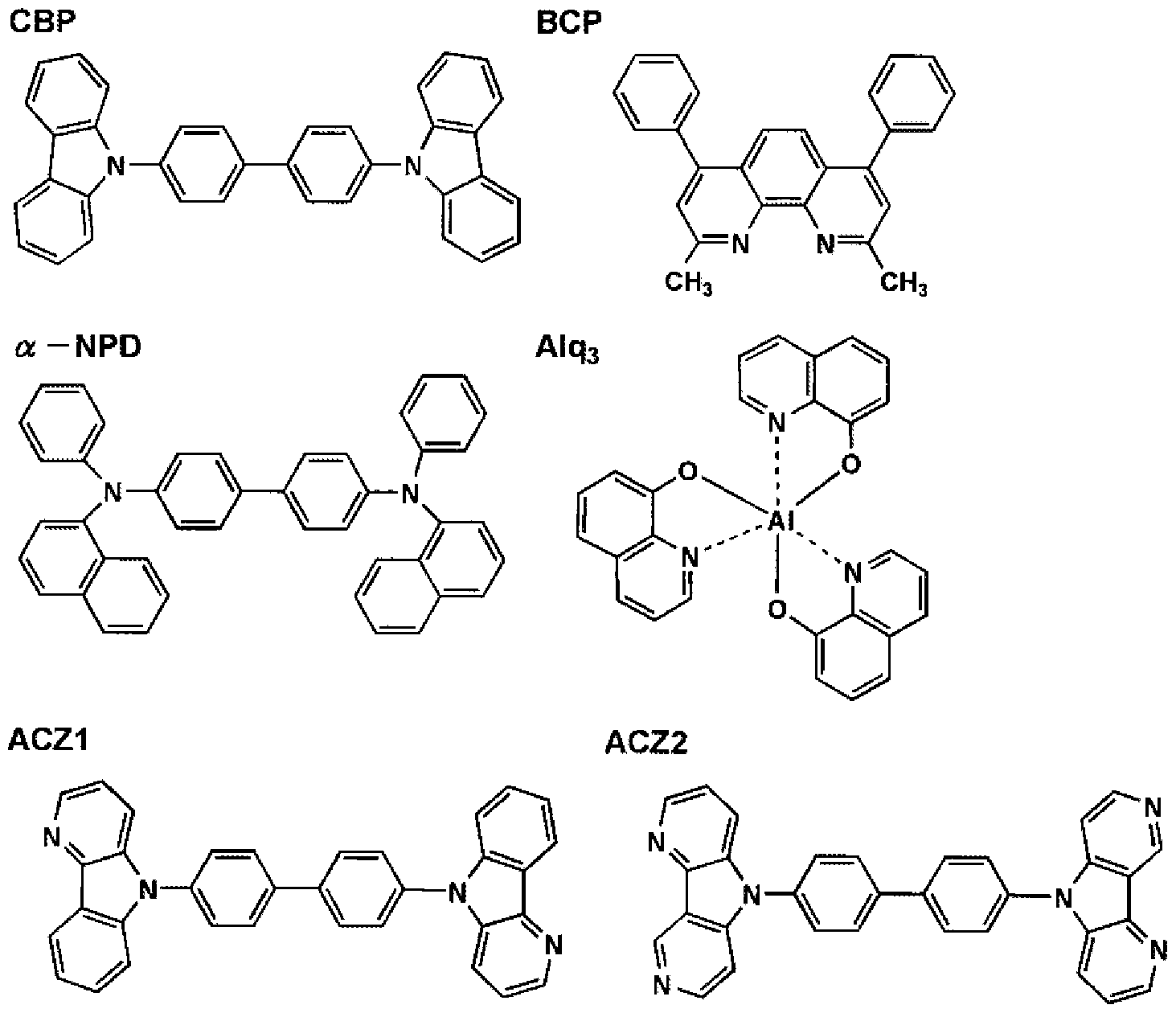
[0295] 〔有機EL素子OLED1— 2〜1 20の作製〕 [Fabrication of organic EL elements OLED1-2—120]
上記有機 EL素子 OLED1— 1の作製において、表 1に記載のように発光ドーパント
、発光ホスト、正孔阻止材料を変更した以外は、同様にして有機 EL素子 OLED1— 2〜 1— 20を作製した。 In the preparation of the organic EL device OLED1-1, as shown in Table 1, the light emitting dopant The organic EL elements OLED1-2 to 1-20 were prepared in the same manner except that the light emitting host and hole blocking material were changed.
[0296] 《有機 EL素子の評価》 [0296] << Evaluation of organic EL elements >>
得られた有機 EL素子 OLED1— 1〜1 20につ 、て下記のような評価を行った。 The obtained organic EL elements OLED1-1 to 120 were evaluated as follows.
[0297] (外部取り出し量子効率の測定) [0297] (Measurement of external extraction quantum efficiency)
有機 EL素子 OLED1— 1〜1— 20を、室温(約 23〜25°C)、 2. 5mAZcm2の定 電流条件下による点灯を行い、点灯開始直後の発光輝度 (L) [cdZm2]を測定する ことにより外部取り出し量子効率( r? )を算出した。ここで、発光輝度の測定は、 CS - 1000 (コ-カミノルタセンシング社製)を用いた。なお、外部取り出し量子効率は、有 機 EL素子 OLED1— 1を 100とした時の相対値で表した。 The organic EL elements OLED1-1 to 20 are turned on at room temperature (approximately 23 to 25 ° C) and under a constant current condition of 2.5 mAZcm 2 , and the emission luminance (L) [cdZm 2 ] immediately after the start of lighting is calculated. The external extraction quantum efficiency (r?) Was calculated by measurement. Here, CS-1000 (manufactured by Co-Kaminolta Sensing Co., Ltd.) was used for the measurement of light emission luminance. The external extraction quantum efficiency is expressed as a relative value when the organic EL element OLED1-1 is set to 100.
[0298] (発光寿命の測定) [0298] (Measurement of luminous lifetime)
有機 EL素子 OLED1— 1〜1 20を、室温下、 2. 5mAZcm2の定電流条件下に よる連続点灯を行い、初期輝度の半分の輝度になるのに要する時間( τ The time required for the organic EL element OLED1—1 to 120 to be lit continuously at room temperature under a constant current condition of 2.5 mAZcm 2 to reach half the initial brightness (τ
1/2 )を測定し た。なお、発光寿命は、有機 EL素子 OLED 1—1を 100とした時の相対値で表した。 1/2) was measured. The light emission lifetime is expressed as a relative value when the organic EL element OLED 1-1 is set to 100.
[0299] 以上により得られた結果を、表 1に示す。 [0299] Table 1 shows the results obtained as described above.
[0300] [表 1]
[0300] [Table 1]
有機 EL 発光 発光 外部取り出し 発光寿命 OLED emission Emission External extraction Emission life
正孔阻止材料 備 考 素子 No. ホス卜 ドーパント 量子効率 <,て ) Hole blocking material Remarks Element No. Phosphorus dopant Quantum efficiency
OLEDI— 1 CBP lr-12 BCP 100 100 比 較 OLEDI— 1 CBP lr-12 BCP 100 100 Comparison
OLEDI -2 CBP lr-11 BCP 102 103 比 較OLEDI -2 CBP lr-11 BCP 102 103 Comparison
OLEDI -3 CBP 2 BCP 122 198 本発明OLEDI -3 CBP 2 BCP 122 198
OLEDI - - CBP 6 BCP 128 203 本発明OLEDI--CBP 6 BCP 128 203 The present invention
OLEDt-5 CBP 10 BCP 126 190 本発明OLEDt-5 CBP 10 BCP 126 190 The present invention
OLEDI -6 CBP 11 BCP 124 197 本発明OLEDI -6 CBP 11 BCP 124 197 The present invention
OLEOI-7 CBP 20 BCP 120 206 本発明OLEOI-7 CBP 20 BCP 120 206 The present invention
0し EDt -8 CBP 30 BCP 128 195 本発明0 EDt -8 CBP 30 BCP 128 195
OLEDI -9 ACZ1 41 BCP 136 220 本発明OLEDI -9 ACZ1 41 BCP 136 220 The present invention
OLEDI -10 ACZ1 48 BCP 133 218 本発明OLEDI -10 ACZ1 48 BCP 133 218
OLEDI -11 ACZ2 39 BCP 131 230 本発明OLEDI -11 ACZ2 39 BCP 131 230 The present invention
OLEDI -12 ACZ2 53 BCP 136 233 本発明OLEDI -12 ACZ2 53 BCP 136 233
OLEDI -13 CBP 33 ACZ1 140 244 本発明OLEDI -13 CBP 33 ACZ1 140 244 The present invention
OLEDI—,4 CBP 38 ACZ2 139 250 本発明OLEDI—, 4 CBP 38 ACZ2 139 250 The present invention
OLEDI— 15 CBP 86 BCP 118 187 本発明OLEDI— 15 CBP 86 BCP 118 187 The present invention
OLEDI— 16 CBP 93 BCP 117 183 本発明OLEDI—16 CBP 93 BCP 117 183
OLED!-17 ACZ1 82 BCP 130 210 本発明OLED! -17 ACZ1 82 BCP 130 210 The present invention
OLEDI— 18 ACZ2 83 BCP 132 213 本発明OLEDI—18 ACZ2 83 BCP 132 213 The present invention
0LE0t~19 CBP 87 ACZ1 139 231 本発明0LE0t ~ 19 CBP 87 ACZ1 139 231 The present invention
OLEDI一 20 CBP 90 ACZ2 137 228 本発明 OLEDI 20 CBP 90 ACZ2 137 228 The present invention
[0301] 表 1に記載の結果より明らかな様に、本発明に係るオルトメタル錯体を用いて作製 した有機 EL素子は、比較有機 EL素子に比べ、高い発光効率と発光寿命の長寿命 化が達成できることが明らかである。 [0301] As is clear from the results shown in Table 1, the organic EL device produced using the ortho metal complex according to the present invention has higher luminous efficiency and longer lifetime than the comparative organic EL device. Clearly it can be achieved.
[0302] 更にカルボリン誘導体または該カルボリン誘導体のカルボリン環を構成する炭化水 素環の炭素原子の少なくとも一つが、更に窒素原子で置換されている環構造を有す る誘導体を発光層に併用することにより、またカルボリン誘導体または該カルボリン誘 導体のカルボリン環を構成する炭化水素環の炭素原子の少なくとも一つが、更に窒 素原子で置換されている環構造を有する誘導体を正孔阻止層に使用することにより 、更に本発明に記載の効果の向上が得られることを確認することができた。 [0302] Further, a carboline derivative or a derivative having a ring structure in which at least one carbon atom of the hydrocarbon ring constituting the carboline ring of the carboline derivative is further substituted with a nitrogen atom is used in the light emitting layer. In addition, a carboline derivative or a derivative having a ring structure in which at least one of the carbon atoms of the hydrocarbon ring constituting the carboline ring of the carboline derivative is further substituted with a nitrogen atom is used for the hole blocking layer. Thus, it was confirmed that the improvement of the effect described in the present invention was obtained.
[0303] 実施例 2 [0303] Example 2
《フルカラー表示装置の作製》 <Production of full-color display device>
(青色発光素子の作製) (Production of blue light-emitting elements)
実施例 1に記載の有機 EL素子 OLED1— 4を青色発光素子として用いた。 The organic EL device OLED1-4 described in Example 1 was used as a blue light emitting device.
[0304] (緑色発光素子の作製)
実施例 1に記載の有機 EL素子 OLED1— 4の作製において、 Ir— 12に代えて、緑 色発光ドーパントとして Ir—1を用いた以外は同様にして、緑色発光素子を作製した [0304] (Production of green light-emitting element) In the production of the organic EL device OLED1-4 described in Example 1, a green light emitting device was produced in the same manner except that Ir-1 was used as a green light emitting dopant instead of Ir-12.
[0305] (赤色発光素子の作製) [0305] (Production of red light-emitting element)
実施例 1に記載の有機 EL素子 OLED1— 4の作製において、 Ir— 12に代えて、赤 色発光ドーパントとして Ir— 9を用いた以外は同様にして、赤色発光素子を作製した In the production of the organic EL device OLED1-4 described in Example 1, a red light emitting device was produced in the same manner except that Ir-9 was used as a red light emitting dopant instead of Ir-12.
[0306] 上記で作製した赤色、緑色、青色発光の各有機 EL素子を同一基板上に並置し、 図 1に記載のような形態を有するアクティブマトリックス方式フルカラー表示装置を作 製し、図 2には作製した前記表示装置の表示部 Aの模式図のみを示した。即ち、同 一基板上に複数の走査線 5及びデータ線 6を含む配線部と並置した複数の画素 3 ( 発光の色が赤領域の画素、緑領域の画素、青領域の画素等)とを有し、配線部の走 查線 5及び複数のデータ線 6はそれぞれ導電材料からなり、走査線 5とデータ線 6は 格子状に直交して、直交する位置で画素 3に接続している(詳細は図示せず)。前記 複数画素 3はそれぞれの発光色に対応した有機 EL素子、アクティブ素子であるスィ ツチングトランジスタと駆動トランジスタそれぞれが設けられたアクティブマトリックス方 式で駆動されており、走査線 5から走査信号が印加されるとデータ線 6から画像デー タ信号を受け取り、受け取った画像データに応じて発光する。この様に各赤、緑、青 の画素を適宜、並置することによって、フルカラー表示装置を作製した。 [0306] The red, green, and blue light-emitting organic EL elements produced above were juxtaposed on the same substrate to produce an active matrix type full-color display device having the configuration shown in Fig. 1, and Fig. 2 Shows only a schematic diagram of the display portion A of the display device thus fabricated. That is, a plurality of pixels 3 (light emission color is a red region pixel, a green region pixel, a blue region pixel, etc.) juxtaposed with a wiring portion including a plurality of scanning lines 5 and data lines 6 on the same substrate. The scanning line 5 and the plurality of data lines 6 in the wiring part are each made of a conductive material, and the scanning lines 5 and the data lines 6 are orthogonal to each other in a grid pattern and are connected to the pixels 3 at orthogonal positions ( Details are not shown). The plurality of pixels 3 are driven by an active matrix system provided with an organic EL element corresponding to each emission color, a switching transistor which is an active element, and a driving transistor, and a scanning signal is applied from a scanning line 5. Then, an image data signal is received from the data line 6 and light is emitted according to the received image data. In this way, a full-color display device was produced by appropriately juxtaposing the red, green, and blue pixels.
[0307] 該フルカラー表示装置を駆動することにより、発光輝度が高ぐ高耐久性を有し、且 つ鮮明なフルカラー動画表示が得られることを確認することができた。 [0307] It was confirmed that by driving the full-color display device, it was possible to obtain a clear full-color moving image display having high durability with high emission luminance.
[0308] 実施例 3 [0308] Example 3
《フルカラー表示装置の作製》 <Production of full-color display device>
実施例 2に記載のフルカラー表示装置の作製において、青色発光素子である有機 EL素子 OLED1— 4に代えて、有機 EL素子 OLED1— 6を用いた以外は、実施例 2 と同様にしてフルカラー表示装置を作製した。該フルカラー表示装置を駆動すること により、発光輝度が高ぐ高耐久性を有し、且つ鮮明なフルカラー動画表示が得られ ることがわかった。
[0309] 実施例 4 In the production of the full-color display device described in Example 2, the full-color display device is the same as Example 2 except that the organic EL element OLED1-6 is used in place of the organic EL element OLED1-4 that is a blue light emitting element. Was made. It has been found that by driving the full-color display device, a clear full-color moving image display having high durability with high emission luminance and high brightness can be obtained. [0309] Example 4
《フルカラー表示装置の作製》 <Production of full-color display device>
実施例 2に記載のフルカラー表示装置の作製において、青色発光素子である有機 EL素子 OLED1— 4に代えて、有機 EL素子 OLED1— 13を用いた以外は、実施例 2と同様にしてフルカラー表示装置を作製した。該フルカラー表示装置を駆動するこ とにより、発光輝度が高ぐ高耐久性を有し、且つ鮮明なフルカラー動画表示が得ら れることがわかった。 In the production of the full-color display device described in Example 2, a full-color display device was obtained in the same manner as in Example 2 except that the organic EL element OLED1-13 was used instead of the organic EL element OLED1-4, which is a blue light emitting element. Was made. It has been found that by driving the full-color display device, it is possible to obtain a clear full-color moving image display having high durability with high light emission luminance.
[0310] 実施例 5 [0310] Example 5
《フルカラー表示装置の作製》 <Production of full-color display device>
実施例 2に記載のフルカラー表示装置の作製において、青色発光素子である有機 EL素子 OLED1— 4に代えて、有機 EL素子 OLED1— 14を用いた以外は、実施例 2と同様にしてフルカラー表示装置を作製した。該フルカラー表示装置を駆動するこ とにより、発光輝度が高ぐ高耐久性を有し、且つ鮮明なフルカラー動画表示が得ら れることがわかった。 In the production of the full-color display device described in Example 2, a full-color display device was obtained in the same manner as in Example 2 except that the organic EL element OLED1-14 was used instead of the organic EL element OLED1-4 that is a blue light emitting element. Was made. It has been found that by driving the full-color display device, it is possible to obtain a clear full-color moving image display having high durability with high light emission luminance.
[0311] 実施例 6 [0311] Example 6
《白色発光素子及び白色照明装置の作製》 << Preparation of white light emitting element and white lighting device >>
実施例 1に記載の透明電極基板の電極を 20mm X 20mmにパターユングし、その 上に実施例 1と同様に正孔注入/輸送層として a— NPDを 25nmの厚さで製膜し、 更に CBPの入った前記加熱ボートと本発明化合物 20の入ったボート及び Ir 9の入 つたボートをそれぞれ独立に通電して、発光ホストである CBPと発光ドーパントである 本発明の例示化合物 20及び Ir— 9の蒸着速度が 100 : 5 : 0. 6になるように調節し、 膜厚 30nmの厚さになるように蒸着し、発光層を設けた。 The electrode of the transparent electrode substrate described in Example 1 was patterned to 20 mm × 20 mm, and then a-NPD was formed to a thickness of 25 nm as a hole injection / transport layer in the same manner as in Example 1, The heated boat containing CBP, the boat containing Compound 20 of the present invention, and the boat containing Ir 9 were energized independently, and CBP as a light emitting host and Illustrative Compound 20 of the present invention as Ir and a light emitting dopant and Ir— The deposition rate of 9 was adjusted to 100: 5: 0.6, deposition was performed to a thickness of 30 nm, and a light emitting layer was provided.
[0312] 次 、で、 BCPを lOnm製膜して正孔阻止層を設けた。更に Alqを 40nmで製膜し [0312] Next, BCP was formed into an lOnm film to provide a hole blocking layer. Furthermore, Alq was deposited at 40nm.
3 Three
電子輸送層を設けた。 An electron transport layer was provided.
[0313] 次に、実施例 1と同様に電子注入層の上にステンレス鋼製の透明電極とほぼ同じ 形状の正方形穴あきマスクを設置し、陰極バッファ一層としてフッ化リチウム 0. 5nm 及び陰極としてアルミニウム 150nmを蒸着製膜した。 [0313] Next, as in Example 1, a square perforated mask having the same shape as the transparent electrode made of stainless steel was placed on the electron injection layer, and lithium fluoride 0.5 nm as a cathode buffer layer and a cathode as a cathode buffer layer. Aluminum 150 nm was deposited.
[0314] この素子を、実施例 1と同様な方法及び同様な構造の封止缶を具備させ平面ラン
プを作製した。図 5、 6に平面ランプの模式図を示した。図 5に概略図を、図 6に断面 図を示す。この平面ランプに通電したところほぼ白色の光が得られ、照明装置として 使用できることがわかった。 [0314] This element was provided with a sealing can having the same method and the same structure as in Example 1, and a planar run was performed. Made a tape. Figures 5 and 6 show schematic diagrams of flat lamps. Figure 5 shows a schematic diagram, and Figure 6 shows a cross-sectional view. When this flat lamp was energized, almost white light was obtained, indicating that it can be used as a lighting device.
[0315] 実施例 7 [0315] Example 7
《白色発光素子及び白色照明装置の作製》 << Preparation of white light emitting element and white lighting device >>
実施例 6の白色発光素子の作製において、本発明の例示化合物 20を、例示化合 物 30に変更した以外は、実施例 6と同様にして白色照明装置を作製した。この平面 ランプに通電したところほぼ白色の光が得られ、照明装置として使用できることがわ かった。 A white lighting device was produced in the same manner as in Example 6 except that the exemplified compound 20 of the present invention was changed to the exemplified compound 30 in the production of the white light emitting device of Example 6. When this flat lamp was energized, almost white light was obtained and it was found that it could be used as a lighting device.
[0316] 実施例 8 [0316] Example 8
《白色発光素子及び白色照明装置の作製》 << Preparation of white light emitting element and white lighting device >>
実施例 6の白色発光素子の作製において、本発明の例示化合物 20を、例示化合 物 39に変更した以外は、実施例 6と同様にして白色照明装置を作製した。この平面 ランプに通電したところほぼ白色の光が得られ、照明装置として使用できることがわ かった。 A white lighting device was produced in the same manner as in Example 6 except that the exemplified compound 20 of the present invention was changed to the exemplified compound 39 in the production of the white light emitting device of Example 6. When this flat lamp was energized, almost white light was obtained and it was found that it could be used as a lighting device.
[0317] 実施例 9 [0317] Example 9
《塗布法による白色発光素子及び白色照明装置の作製》 << Preparation of white light emitting element and white illumination device by coating method >>
25mm X 25mm X O. 5mmのガラス支持基板上に直流電源を用い、スパッタ法に てインジウム錫酸ィ匕物(ITO、インジウム Ζ錫 = 95Ζ5モル比)の陽極を形成した (厚 み 200nm)。この陽極の表面抵抗は 10 Ω ロであった。これにポリビュルカルバゾ ール (正孔輸送性バインダーポリマー) /本発明の例示化合物 6 (青発光性オルトメ タル錯体) /トリス(2—フエ-ノレピリジン)イリジウム錯体 (緑発光性オルトメタル錯体: I r 1) Zビス(2—ベンゾチォフェン [b]— 2—イノレーピリジン)ァセチノレアセトナ トイ リジゥム錯体 (赤発光性オルトメタル錯体: Ir— 9) Z2— (4—ビフエ-リル)—5— (4 t ブチルフエ-ル) 1, 3, 4ーォキサジァゾール(電子輸送材) =200Z2Z5 /2/50質量比を溶解したジクロロエタン溶液をスピンコ―タ—で塗布し、 lOOnmの 発光層を得た。 An anode of indium stannate (ITO, indium Ζ tin = 95 Ζ 5 mole ratio) was formed on a glass support substrate of 25 mm X 25 mm X O. 5 mm using a DC power source by sputtering (thickness 200 nm). The surface resistance of this anode was 10 Ω. Polyburecarbazole (hole transporting binder polymer) / Exemplary compound 6 of the present invention (blue light emitting orthometal complex) / Tris (2-phenol-pyridine) iridium complex (green light emitting orthometal complex): I r 1) Z bis (2-benzothiophene [b] — 2-inolepyridine) acetinoreacetonato lysium complex (red luminescent ortho-metal complex: Ir— 9) Z2— (4-biphenyl) — 5— (4 t-butylphenol) 1, 3, 4-oxadiazole (electron transport material) = 200Z2Z5 / 2/50 mass ratio dissolved dichloroethane solution was applied with a spin coater, lOOnm emission A layer was obtained.
[0318] この有機化合物層の上にパターユングしたマスク(発光面積が 5mm X 5mmとなる
マスク)を設置し、蒸着装置内で陰極バッファ一層としてフッ化リチウム 0. 5nm及び 陰極としてアルミニウム 150nmを蒸着して陰極を設けた。陽極、陰極よりそれぞれァ ルミ-ゥムのリード線を出して発光素子を作製した。該素子を窒素ガスで置換したグ 口 ブボックス内に入れ、ガラス製の封止容器で紫外線硬化型接着剤 (長瀬チバ製 、 XNR5493)を用いて封止して平面ランプを作製した。この平面ランプに通電したと ころほぼ白色の光が得られ、照明装置として使用できることがわ力つた。 [0318] A mask patterned on this organic compound layer (light emission area is 5mm x 5mm) In the vapor deposition apparatus, 0.5 nm of lithium fluoride was deposited as a cathode buffer layer and 150 nm of aluminum was deposited as a cathode to provide a cathode. A light-emitting device was fabricated by emitting aluminum lead wires from the anode and cathode, respectively. The device was placed in a glove box substituted with nitrogen gas, and sealed with a glass sealing container using an ultraviolet curable adhesive (XNR5493, manufactured by Nagase Ciba) to produce a flat lamp. When this flat lamp was energized, almost white light was obtained, which proved to be usable as a lighting device.
[0319] 実施例 10 [0319] Example 10
《塗布法による白色発光素子及び白色照明装置の作製》 << Preparation of white light emitting element and white illumination device by coating method >>
実施例 9の白色発光素子の作製において、本発明の例示化合物 6を、例示化合物 11に変更した以外は、実施例 9と同様にして白色照明装置を作製した。この平面ラ ンプに通電したところほぼ白色の光が得られ、照明装置として使用できることがわか つた o A white lighting device was produced in the same manner as in Example 9, except that Example Compound 6 of the present invention was changed to Example Compound 11 in the production of the white light emitting device of Example 9. When this flat lamp is energized, almost white light is obtained and it can be used as a lighting device.
[0320] 実施例 11《塗布法による白色発光素子及び白色照明装置の作製》 Example 11 << Preparation of White Light-Emitting Element and White Lighting Device by Coating Method >>
実施例 9の白色発光素子の作製において、本発明の例示化合物 6を、例示化合物 52に変更した以外は、実施例 9と同様にして白色照明装置を作製した。この平面ラ ンプに通電したところほぼ白色の光が得られ、照明装置として使用できることがわか つた o A white lighting device was produced in the same manner as in Example 9, except that Example Compound 6 of the present invention was changed to Example Compound 52 in the production of the white light-emitting device of Example 9. When this flat lamp is energized, almost white light is obtained and it can be used as a lighting device.
[0321] 実施例 12 [0321] Example 12
《塗布法による白色発光素子及び白色照明装置の作製》 << Preparation of white light emitting element and white illumination device by coating method >>
25mm X 25mm X O. 5mmのガラス支持基板上に直流電源を用い、スパッタ法に てインジウム錫酸ィ匕物(ITO、インジウム Ζ錫 = 95Ζ5モル比)の陽極を形成した (厚 み 200nm)。この陽極の表面抵抗は 10 Ω ロであった。これにポリビュルカルバゾ ール (正孔輸送性バインダーポリマー) ZACZ1 (正孔輸送制御材) /本発明の例示 化合物 41 (青発光性オルトメタル錯体) Zトリス(2 フエ-ルビリジン)イリジウム錯体 (緑発光性オルトメタル錯体: Ir— 1 ) Zビス ( 2 -ベンゾチォフェン [b]— 2—ィル一ピ リジン)ァセチルァセトナ―トイリジウム錯体 (赤発光性オルトメタル錯体: Ir— 9) /2 — (4 ビフエ-リル)— 5— (4— t—ブチルフエ-ル)— 1, 3, 4—ォキサジァゾ—ル( 電子輸送材) = 150/50/2/5/2/50質量比を溶解したジクロロエタン溶液をス
ビンコ—タ—で塗布し、 lOOnmの発光層を得た。 An anode of indium stannate (ITO, indium Ζ tin = 95 Ζ 5 mole ratio) was formed on a glass support substrate of 25 mm X 25 mm X O. 5 mm using a DC power source by sputtering (thickness 200 nm). The surface resistance of this anode was 10 Ω. Polyburcarbazole (Hole transporting binder polymer) ZACZ1 (Hole transport control material) / Exemplary compound of the present invention Compound 41 (Blue light emitting orthometal complex) Z Tris (2 phenol-lysine) iridium complex ( Green luminescent orthometal complex: Ir— 1) Z bis (2 -benzothiophene [b] — 2-yl pyridine) acetylylacetonate-toiridium complex (red luminescent orthometal complex: Ir— 9) / 2 — ( 4 Biphenyl) — 5— (4— t-Butyl phenol) — 1, 3, 4-Oxadiazole (electron transport material) = dichloroethane in which 150/50/2/5/2/50 mass ratio is dissolved Solution Coating with a bin coater gave a light emitting layer of lOOnm.
[0322] この有機化合物層の上に、ノターユングしたマスク(発光面積が 5mm X 5mmとな るマスク)を設置し、蒸着装置内で陰極バッファ一層としてフッ化リチウム 0. 5nm及び 陰極としてアルミニウム 150nmを蒸着して陰極を設けた。陽極、陰極よりそれぞれァ ルミ-ゥムのリード線を出して発光素子を作製した。該素子を窒素ガスで置換したグ 口 ブボックス内に入れ、ガラス製の封止容器で紫外線硬化型接着剤 (長瀬チバ製 、 XNR5493)を用いて封止して平面ランプを作製した。この平面ランプに通電したと ころほぼ白色の光が得られ、照明装置として使用できることを確認することができた。 [0322] A notched mask (a mask with a light emitting area of 5 mm x 5 mm) was placed on this organic compound layer, and lithium fluoride 0.5 nm as the cathode buffer layer and aluminum 150 nm as the cathode in the vapor deposition system. The cathode was provided by vapor deposition. A light-emitting device was fabricated by emitting aluminum lead wires from the anode and cathode, respectively. The device was placed in a glove box substituted with nitrogen gas, and sealed with a glass sealing container using an ultraviolet curable adhesive (XNR5493, manufactured by Nagase Ciba) to produce a flat lamp. When this flat lamp was energized, almost white light was obtained, confirming that it could be used as a lighting device.
[0323] 実施例 13 [0323] Example 13
《白色発光素子及び白色照明装置の作製》 << Preparation of white light emitting element and white lighting device >>
実施例 12の白色発光素子の作製において、本発明の例示化合物 41を、例示化 合物 39に変更した以外は、実施例 12と同様にして白色照明装置を作製した。この 平面ランプに通電したところほぼ白色の光が得られ、照明装置として使用できること がわかった。 A white lighting device was produced in the same manner as in Example 12 except that Example Compound 41 of the present invention was changed to Example Compound 39 in the production of the white light-emitting device of Example 12. When this flat lamp was energized, almost white light was obtained, indicating that it could be used as a lighting device.
[0324] 実施例 14 [0324] Example 14
《白色発光素子及び白色照明装置の作製》 << Preparation of white light emitting element and white lighting device >>
実施例 12の白色発光素子の作製において、正孔輸送制御材 ACZ1を ACZ2に変 更した以外は、実施例 12と同様にして白色照明装置を作製した。この平面ランプに 通電したところほぼ白色の光が得られ、照明装置として使用できることがわ力つた。 A white lighting device was produced in the same manner as in Example 12 except that the hole transport control material ACZ1 was changed to ACZ2 in the production of the white light emitting device of Example 12. When this flat lamp was energized, almost white light was obtained, which proved to be usable as a lighting device.
[0325] 実施例 15 [0325] Example 15
《有機 EL素子 OLED2— 1〜2— 13の作製》 << Production of organic EL elements OLED2-1—1-2-13 >>
実施例 1に記載の有機 EL素子 OLED1— 1の作製において、発光ドーパントを Ir 1に変更し、正孔阻止材料を表 2に記載のように変更した以外は同様にして、有機 EL素子 OLED2— 1〜2— 13を作製した。得られた各々の有機 EL素子の外部取り 出し量子効率、発光寿命の測定を実施例 1に記載の方法と同様にして行った。この 時、いずれも、有機 EL素子 OLED2— 1の値を 100として、各有機 EL素子の値を相 対値で表した。得られた結果を表 2に示す。 In the production of the organic EL device OLED1-1 described in Example 1, the organic EL device OLED2— was similarly prepared except that the luminescent dopant was changed to Ir 1 and the hole blocking material was changed as shown in Table 2. 1-2-13 were produced. Measurement of the external extraction quantum efficiency and emission lifetime of each obtained organic EL device was carried out in the same manner as described in Example 1. At this time, the value of the organic EL element OLED2-1 was assumed to be 100, and the value of each organic EL element was expressed as a relative value. Table 2 shows the results obtained.
[0326] [表 2]
有機 EL 外部取り出し 発光奢 [0326] [Table 2] External take-out of organic EL
正孔阻止材料 備 考 Hole blocking material Remarks
素子 No. 量子効率 ( Γ Element No. Quantum efficiency (Γ
0LED2-) BCP 100 100 比 較 0LED2-) BCP 100 100 Comparison
0LED2-2 2 116 250 本発明 0LED2-2 2 116 250 The present invention
0LED2-3 6 115 25! 本発明 0LED2-3 6 115 25! The present invention
0LED2-4 15 117 255 本発明 0LED2-4 15 117 255 The present invention
0LED2-5 21 116 254 本発明 0LED2-5 21 116 254 The present invention
0LED2-6 31 115 253 本発明 0LED2-6 31 115 253 The present invention
0LED2-7 40 117 252 本発明 0LED2-7 40 117 252 The present invention
0LED2-8 52 115 251 本発明 0LED2-8 52 115 251 The present invention
OLE02-9 64 118 253 本発明 OLE02-9 64 118 253 The present invention
0 67 113 247 本発明 0 67 113 247 The present invention
74 116 250 本発明 74 116 250 The present invention
0LED2-12 84 115 248 本発明 0LED2-12 84 115 248 The present invention
0LED2-13 96 117 246 本発明 表 2から、本発明の有機 EL素子材料を正孔阻止材料に用いた有機 EL素子は、比 較素子に比べ、高い発光効率と発光寿命が得られることがわかった。なお、本発明 の有機 EL素子の発光色は全て緑色だった。
0LED2-13 96 117 246 Invention Table 2 shows that an organic EL device using the organic EL device material of the present invention as a hole blocking material can obtain higher luminous efficiency and lifetime than a comparative device. It was. The emission color of the organic EL device of the present invention was all green.
Claims
[化 1] [Chemical 1]
一般式 (Z)
 Formula (Z)
〔式中、 Xは 0、 S、 SOまたは SOを表し、 Xは 2価の基または単結合を表す。 Rは置 [Wherein, X represents 0, S, SO or SO, and X represents a divalent group or a single bond. R is set
2 1 a 換基を表す。 R 2 1 a represents a substituent. R
bは水素原子または置換基を表す。 Lは窒素原子と共に 5〜7員の芳 香族複素環を形成する。 Mは元素周期表における第 8族〜第 10族の金属元素を表 す。〕 b represents a hydrogen atom or a substituent. L forms a 5- to 7-membered aromatic heterocycle with the nitrogen atom. M represents a metal element of Group 8 to Group 10 in the periodic table. ]
前記一般式 (Z)で表される部分構造が、下記一般式(1)で表される部分構造であ ることを特徴とする請求の範囲第 1項に記載の有機エレクト口ルミネッセンス素子材料 2. The organic electroluminescence device material according to claim 1, wherein the partial structure represented by the general formula (Z) is a partial structure represented by the following general formula (1):
[化 2] [Chemical 2]
一般式 ("
 General formula ("
〔式中、 X は 0、 S、 SOまたは SOを表し、 Rは置換基を表す。 Rは水素原子または [Wherein, X represents 0, S, SO or SO, and R represents a substituent. R is a hydrogen atom or
10 2 1 2 10 2 1 2
置換基を表す。 X 、X 、X 、X は各々 C、C— R 、N、N— R 、 Oまたは Sを表し、 Represents a substituent. X 1, X 2, X 3 and X 3 each represent C, C—R, N, N—R, O or S;
11 12 13 14 11 11 且つ窒素原子と共に 5員の芳香族複素環を形成する。 R は水素原子または置換基
を表す。 Mは元素周期表における第 8族〜第 10族の金属元素を表す。〕 前記一般式 (Z)で表される部分構造が、下記一般式 (2)で表される部分構造であ ることを特徴とする請求の範囲第 1項に記載の有機エレクト口ルミネッセンス素子材料 11 12 13 14 11 11 and forms a 5-membered aromatic heterocycle with the nitrogen atom. R is a hydrogen atom or a substituent Represents. M represents a metal element of Group 8 to Group 10 in the periodic table. The organic electroluminescent device material according to claim 1, wherein the partial structure represented by the general formula (Z) is a partial structure represented by the following general formula (2):
[化 3] 一般式 (2)
 [Chemical formula 3] General formula (2)
〔式中、 X は 0、 S、 SOまたは SOを表し、 Rは置換基を表す。 Rは水素原子または [Wherein, X represents 0, S, SO or SO, and R represents a substituent. R is a hydrogen atom or
20 2 3 4 20 2 3 4
置換基を表す。 X 、X 、X 、X は各々 C—R または Nを表し、且つ炭素原子、窒 Represents a substituent. X 1, X 2, X 3 and X each represent C—R or N, and a carbon atom, nitrogen
21 22 23 24 21 21 22 23 24 21
素原子と共に 6員の芳香族複素環を形成する。 R は水素原子または置換基を表す Forms a 6-membered aromatic heterocycle with the elementary atoms. R represents a hydrogen atom or a substituent
21 twenty one
。 Mは元素周期表における第 8族〜第 10族の金属元素を表す。〕 . M represents a metal element of Group 8 to Group 10 in the periodic table. ]
前記一般式 (Z)で表される部分構造が、下記一般式 (3)で表される部分構造であ ることを特徴とする請求の範囲第 1項に記載の有機エレクト口ルミネッセンス素子材料 2. The organic electroluminescent device material according to claim 1, wherein the partial structure represented by the general formula (Z) is a partial structure represented by the following general formula (3):
[化 4] [Chemical 4]
—般式 (3> —General formula (3>

30 2 5 6 置換基を表す。 X 、X 、X 、X は各々 C、C— R 、N、N— R 、 Oまたは Sを表し、 30 2 5 6 represents a substituent. X 1, X 2, X 3 and X 3 each represent C, C—R, N, N—R, O or S;
31 32 33 34 31 31 31 32 33 34 31 31
且つ窒素原子と共に 5員の芳香族複素環を形成する。 R は水素原子または置換基 It forms a 5-membered aromatic heterocycle with the nitrogen atom. R is a hydrogen atom or a substituent
31 31
を表す。 Xは 0、 S、 CH、 CHR、 C (R)、 NR、 PR、 Si (R)、 C = 0、 C=NR、 SO、 Represents. X is 0, S, CH, CHR, C (R), NR, PR, Si (R), C = 0, C = NR, SO,
0 2 2 2 0 2 2 2
SOを表す。 Rはアルキル基、シクロアルキル基、アルケニル基、ァリール基、複素環 Represents SO. R is an alkyl group, a cycloalkyl group, an alkenyl group, an aryl group, a heterocyclic ring
2 2
基または芳香族複素環基を表す。 Mは元素周期表における第 8族〜第 10族の金属 元素を表す。〕 Represents a group or an aromatic heterocyclic group. M represents a metal element of Group 8 to Group 10 in the periodic table. ]
前記一般式 (Z)で表される部分構造が、下記一般式 (4)で表される部分構造であ ることを特徴とする請求の範囲第 1項に記載の有機エレクト口ルミネッセンス素子材料 2. The organic electroluminescence device material according to claim 1, wherein the partial structure represented by the general formula (Z) is a partial structure represented by the following general formula (4):
[化 5] [Chemical 5]
一般式 (4) General formula (4)

〔式中、 X は 0、 S、 SOまたは SOを表し、 Rは置換基を表す。 Rは水素原子または [Wherein, X represents 0, S, SO or SO, and R represents a substituent. R is a hydrogen atom or
40 2 7 8 置換基を表す。 X 、X 、X 、X は各々 C—R または Nを表し、且つ炭素原子、窒 40 2 7 8 represents a substituent. X 1, X 2, X 3 and X each represent C—R or N, and a carbon atom, nitrogen
41 42 43 44 41 41 42 43 44 41
素原子と共に 6員の芳香族複素環を形成する。 R は水素原子または置換基を表す Forms a 6-membered aromatic heterocycle with the elementary atoms. R represents a hydrogen atom or a substituent
41 41
。 Xは 0、 S、 CH、 CHR、 C (R) 、 NRゝ PR、 Si (R)、 C = 0、 C=NR、 SO、 SOを . X is 0, S, CH, CHR, C (R), NR ゝ PR, Si (R), C = 0, C = NR, SO, SO
0 2 2 2 2 表す。 Rはアルキル基、シクロアルキル基、ァルケ-ル基、ァリール基、複素環基また は芳香族複素環基を表す。 Mは元素周期表における第 8族〜第 10族の金属元素を 表す。〕 0 2 2 2 2 represents. R represents an alkyl group, a cycloalkyl group, an alkyl group, an aryl group, a heterocyclic group or an aromatic heterocyclic group. M represents a metal element of Group 8 to Group 10 in the periodic table. ]
[6] 前記一般式 (2)で表される部分構造が、下記一般式 (5)で表される部分構造であ ることを特徴とする請求の範囲第 3項に記載の有機エレクト口ルミネッセンス素子材料
[化 6] [6] The organic electoluminescence according to claim 3, wherein the partial structure represented by the general formula (2) is a partial structure represented by the following general formula (5): Element material [Chemical 6]
一般
 General
〔式中、 R は置換基を表し、 R は水素原子または置換基を表す。 R と R の少なくと [Wherein, R represents a substituent, and R represents a hydrogen atom or a substituent. At least R and R
51 52 51 52 も一方は電子供与性の置換基または電子吸引性の置換基である。 X は o、 s、 One of 51 52 51 52 is an electron-donating substituent or an electron-withdrawing substituent. X is o, s,
51 so または SOを表す。 R は置換基を表し、 n51は 0〜3から選ばれる整数を表す。 Xaは 51 Represents so or SO. R represents a substituent, and n51 represents an integer selected from 0 to 3. Xa
2 50 2 50
-N (Ra) 、—O—Raまたは— S—Raを表す。 Raはアルキル基、シクロアルキル基、 -N (Ra), —O—Ra or —S—Ra is represented. Ra is an alkyl group, a cycloalkyl group,
2 2
アルケニル基、ァリール基、複素環基または芳香族複素環基を表す。 Xaがー N (Ra )の場合、 2つの Raは同じであっても異なっていてもよい。 Mは元素周期表におけるAn alkenyl group, an aryl group, a heterocyclic group or an aromatic heterocyclic group; When Xa is -N (Ra), the two Ras may be the same or different. M in the periodic table
2 2
第 8族〜第 10族の金属元素を表す。〕 Represents Group 8 to Group 10 metal elements. ]
前記一般式 (4)で表される部分構造が、下記一般式 (6)で表される部分構造であ ることを特徴とする請求の範囲第 5項に記載の有機エレクト口ルミネッセンス素子材料 6. The organic electroluminescent device material according to claim 5, wherein the partial structure represented by the general formula (4) is a partial structure represented by the following general formula (6):
[化 7] 一般式 (6)
 [Chemical formula 7] General formula (6)
〔式中、 R は置換基を表し、 R は水素原子または置換基を表す。 R と R の少なくと [Wherein, R represents a substituent, and R represents a hydrogen atom or a substituent. At least R and R
56 57 56 57 も一方は電子供与性の置換基または電子吸引性の置換基である。 X は One of 56 57 56 57 is an electron-donating substituent or an electron-withdrawing substituent. X is
52 o、 s、 so または SOを表す。 R は置換基を表し、 n52は 0〜3から選ばれる整数を表す。 Xaは 52 represents o, s, so or SO. R represents a substituent, and n52 represents an integer selected from 0 to 3. Xa
2 55 2 55
-N (Ra) 、—O—Raまたは— S—Raを表す。 Raはアルキル基、シクロアルキル基、 -N (Ra), —O—Ra or —S—Ra is represented. Ra is an alkyl group, a cycloalkyl group,
2 2
アルケニル基、ァリール基、複素環基または芳香族複素環基を表す。 Xaがー N (Ra
)の場合、 2つの Raは同じであっても異なっていてもよい。 Xは 0、 S、 CH、 CHR、An alkenyl group, an aryl group, a heterocyclic group or an aromatic heterocyclic group; Xa-N (Ra ), The two Ras may be the same or different. X is 0, S, CH, CHR,
2 0 2 2 0 2
C (R)、 NR、 PR、 Si (R)、 C = 0、 C=NR、 SO、 SOを表す。 Rはアルキル基、シク C (R), NR, PR, Si (R), C = 0, C = NR, SO, SO. R is an alkyl group,
2 2 2 2 2 2
口アルキル基、アルケニル基、ァリール基、複素環基または芳香族複素環基を表す。 It represents a mouth alkyl group, an alkenyl group, an aryl group, a heterocyclic group or an aromatic heterocyclic group.
Mは元素周期表における第 8族〜第 10族の金属元素を表す。〕 M represents a metal element of Group 8 to Group 10 in the periodic table. ]
前記一般式(1)で表される部分構造が、下記一般式 (7A)または一般式 (8A)で表 される部分構造であることを特徴とする請求の範囲第 2項に有機エレクト口ルミネッセ ンス素子材料。 3. The organic electoluminescence device according to claim 2, wherein the partial structure represented by the general formula (1) is a partial structure represented by the following general formula (7A) or the general formula (8A). Element material.
[化 8] [Chemical 8]
—般式 (7A) —般式 (8A) —General formula (7A) —General formula (8A)

〔式中、 X 、X 、X 、X [Where X, X, X, X
61 62 63 64は各々炭素原子または窒素原子を表し、 Q 61 62 63 64 each represents a carbon atom or a nitrogen atom, and Q
1は炭素原子、 X 1 is a carbon atom, X
、 X と共に 5員の芳香族複素環を形成する原子群を表し、 Qは炭素原子、 X 、 X, X represents a group of atoms that form a 5-membered aromatic heterocyclic ring, Q is a carbon atom, X, X
61 62 2 63 6461 62 2 63 64
、窒素原子と共に 5員の芳香族複素環を形成する原子群を表す。 X、 Xは 0、 S、 S Represents a group of atoms that form a 5-membered aromatic heterocycle with the nitrogen atom. X, X is 0, S, S
1 2 1 2
Oまたは SOを表す。 R は置換基を表し、 R は水素原子または置換基を表す。 R 、 Represents O or SO. R represents a substituent, and R represents a hydrogen atom or a substituent. R,
2 15 26 16 2 15 26 16
R 、R 、R はファンデルワールス体積が 20 R 1, R 2 and R have a van der Waals volume of 20
17 25 27 A3以上である置換基を表す。 n61、n617 25 27 A represents a substituent that is 3 or more. n61, n6
2、 n63は 0または 1を表す。但し、 n61 +n62≥lである。 Mは元素周期表における 第 8族〜第 10族の金属元素を表す。〕 2, n63 represents 0 or 1; However, n61 + n62≥l. M represents a metal element of Group 8 to Group 10 in the periodic table. ]
[9] 前記一般式 (2)で表される部分構造が、下記一般式 (7B)または一般式 (8B)で表 される部分構造であることを特徴とする請求の範囲第 3項に有機エレクト口ルミネッセ ンス素子材料。 [9] The organic compound according to claim 3, wherein the partial structure represented by the general formula (2) is a partial structure represented by the following general formula (7B) or the general formula (8B): Electric mouth luminescence element material.
[化 9]
一般式 (8B) [Chemical 9] General formula (8B)

〔式中、 X 、 X 、 X 、 X は各々炭素原子または窒素原子を表し、 Qは炭素原子、 X [Wherein X, X, X and X each represents a carbon atom or a nitrogen atom, Q represents a carbon atom, X
63 63
、 X と共に 6員の芳香族複素環を形成する原子群を表し、 Qは炭素原子、 X 、 X , X represents a group of atoms that form a 6-membered aromatic heterocycle with Q being a carbon atom, X, X
2 2
、窒素原子と共に 6員の芳香族複素環を形成する原子群を表す。 X、 Xは 0、 S、 S Represents a group of atoms that together with the nitrogen atom form a 6-membered aromatic heterocycle. X, X is 0, S, S
2 2
Oまたは SOを表す。 R は置換基を表し、 R は水素原子または置換基を表す。 R 、 Represents O or SO. R represents a substituent, and R represents a hydrogen atom or a substituent. R,
2 15 26 16 2 15 26 16
R 、 R 、 R はファンデルワールス体積が 20 A3以上である置換基を表す。 n61、 n6R 1, R 2 and R 3 each represent a substituent having a van der Waals volume of 20 A 3 or more. n61, n6
17 25 27 17 25 27
2、 n63は 0または 1を表す。但し、 n61 +n62≥lである。 Mは元素周期表における 第 8族〜第 10族の金属元素を表す。〕 2, n63 represents 0 or 1; However, n61 + n62≥l. M represents a metal element of Group 8 to Group 10 in the periodic table. ]
前記一般式 (3)で表される部分構造が、下記一般式 (9A)または一般式(10A)で 表される部分構造であることを特徴とする請求の範囲第 4項に記載の有機エレクト口 ルミネッセンス素子材料。 5. The organic elect according to claim 4, wherein the partial structure represented by the general formula (3) is a partial structure represented by the following general formula (9A) or the general formula (10A): Mouth Luminescence element material.
[化 10] 一般 [Chemical 10] General

〔式中、 X 、 X 、 X 、 X は各々炭素原子または窒素原子を表し、 Qは炭素原子、 X [Wherein X, X, X and X each represents a carbon atom or a nitrogen atom, Q represents a carbon atom, X
71 72 73 74 3 71 72 73 74 3
、 X と共に 5員の芳香族複素環を形成する原子群を表し、 Qは炭素原子、 X 、 X , X represents a group of atoms that form a 5-membered aromatic heterocyclic ring, Q is a carbon atom, X, X
71 72 4 73 7471 72 4 73 74
、窒素原子と共に 5員の芳香族複素環を形成する原子群を表す。 X、 Xは 0、 S、 S Represents a group of atoms that form a 5-membered aromatic heterocycle with the nitrogen atom. X, X is 0, S, S
3 4 3 4
Oまたは SOを表す。 R は置換基を表し、 R は水素原子または置換基を表す。 R 、
R 、R 、R はファンデルワールス体積が 20A3以上である置換基を表す。 n71、 n7Represents O or SO. R represents a substituent, and R represents a hydrogen atom or a substituent. R, R 1, R 2 and R 3 each represent a substituent having a van der Waals volume of 20A 3 or more. n71, n7
37 45 47 37 45 47
2、 n73は 0または 1を表す。但し、 n71 +n72≥lである。 Xは 0、 S、 CH、 CHR、 C 2, n73 represents 0 or 1; However, n71 + n72≥l. X is 0, S, CH, CHR, C
0 2 0 2
(R)、 NR、 PR、 Si (R)、 C = 0、 C=NR、 SO、 SOを表す。 Rはアルキル基、シクロ (R), NR, PR, Si (R), C = 0, C = NR, SO, SO. R is an alkyl group, cyclo
2 2 2 2 2 2
アルキル基、アルケニル基、ァリール基、複素環基または芳香族複素環基を表す。 Mは元素周期表における第 8族〜第 10族の金属元素を表す。〕 Represents an alkyl group, an alkenyl group, an aryl group, a heterocyclic group or an aromatic heterocyclic group; M represents a metal element of Group 8 to Group 10 in the periodic table. ]
前記一般式 (4)で表される部分構造が、下記一般式 (9B)または一般式( 10B)で 表される部分構造であることを特徴とする請求の範囲第 5項に記載の有機エレクト口 ルミネッセンス素子材料。 6. The organic elect according to claim 5, wherein the partial structure represented by the general formula (4) is a partial structure represented by the following general formula (9B) or the general formula (10B): Mouth Luminescence element material.
[化 11] 一般 [Chemical 11] General

〔式中、 X 、X 、X 、X は各々炭素原子または窒素原子を表し、 Qは炭素原子、 X [Wherein, X 1, X 2, X 3, X represent a carbon atom or a nitrogen atom, Q represents a carbon atom, X
71 72 73 74 3 71 72 73 74 3
、 X と共に 6員の芳香族複素環を形成する原子群を表し、 Qは炭素原子、 X 、 X , X represents a group of atoms that form a 6-membered aromatic heterocycle with Q being a carbon atom, X, X
71 72 4 73 7471 72 4 73 74
、窒素原子と共に 6員の芳香族複素環を形成する原子群を表す。 X、 Xは 0、 S、 S Represents a group of atoms that together with the nitrogen atom form a 6-membered aromatic heterocycle. X, X is 0, S, S
3 4 3 4
Oまたは SOを表す。 R は置換基を表し、 R は水素原子または置換基を表す。 R 、 Represents O or SO. R represents a substituent, and R represents a hydrogen atom or a substituent. R,
2 35 46 36 2 35 46 36
R 、R 、R はファンデルワールス体積が 20 A3以上である置換基を表す。 n71、n7R 1, R 2 and R 3 represent a substituent having a van der Waals volume of 20 A 3 or more. n71, n7
37 45 47 37 45 47
2、 n73は 0または 1を表す。但し、 n71 +n72≥lである。 Xは 0、 S、 CH、 CHR、 C 2, n73 represents 0 or 1; However, n71 + n72≥l. X is 0, S, CH, CHR, C
0 2 0 2
(R)、 NR、 PR、 Si (R)、 C = 0、 C=NR、 SO、 SOを表す。 Rはアルキル基、シクロ (R), NR, PR, Si (R), C = 0, C = NR, SO, SO. R is an alkyl group, cyclo
2 2 2 2 2 2
アルキル基、アルケニル基、ァリール基、複素環基または芳香族複素環基を表す。 Mは元素周期表における第 8族〜第 10族の金属元素を表す。〕 Represents an alkyl group, an alkenyl group, an aryl group, a heterocyclic group or an aromatic heterocyclic group; M represents a metal element of Group 8 to Group 10 in the periodic table. ]
[12] 前記一般式 (Z)における Mが、イリジウムまたは白金であることを特徴とする請求の 範囲第 1項に記載の有機エレクト口ルミネッセンス素子材料。 [12] The organic electroluminescence device material according to claim 1, wherein M in the general formula (Z) is iridium or platinum.
[13] 請求の範囲第 1項に記載の有機エレクト口ルミネッセンス素子材料を、構成層の少
なくとも 1層に含有することを特徴とする有機エレクト口ルミネッセンス素子。 [13] The organic electoluminescence device material according to claim 1, wherein An organic electoluminescence device characterized in that it is contained in at least one layer.
[14] 構成層として発光層を有し、該発光層が請求の範囲第 1項に記載の有機エレクト口 ルミネッセンス素子材料を含有することを特徴とする有機エレクト口ルミネッセンス素 子。 [14] An organic electoluminescence device comprising a luminescent layer as a constituent layer, wherein the luminescent layer contains the organic electoluminescence device material according to claim 1.
[15] 請求の範囲第 13項に記載の有機エレクト口ルミネッセンス素子を有することを特徴 とする表示装置。 [15] A display device comprising the organic electoluminescence element according to claim 13.
[16] 請求の範囲第 13項に記載の有機エレクト口ルミネッセンス素子を有することを特徴 とする照明装置。
[16] An illumination device comprising the organic electoluminescence element according to claim 13.
Priority Applications (1)
| Application Number | Priority Date | Filing Date | Title |
|---|---|---|---|
| JP2007510348A JPWO2006103874A1 (en) | 2005-03-29 | 2006-03-06 | ORGANIC ELECTROLUMINESCENT ELEMENT MATERIAL, ORGANIC ELECTROLUMINESCENT ELEMENT, DISPLAY DEVICE AND LIGHTING DEVICE |
Applications Claiming Priority (2)
| Application Number | Priority Date | Filing Date | Title |
|---|---|---|---|
| JP2005094191 | 2005-03-29 | ||
| JP2005-094191 | 2005-03-29 |
Publications (1)
| Publication Number | Publication Date |
|---|---|
| WO2006103874A1 true WO2006103874A1 (en) | 2006-10-05 |
Family
ID=37053141
Family Applications (1)
| Application Number | Title | Priority Date | Filing Date |
|---|---|---|---|
| PCT/JP2006/304234 WO2006103874A1 (en) | 2005-03-29 | 2006-03-06 | Organic electroluminescent device material, organic electroluminescent device, display and illuminating device |
Country Status (2)
| Country | Link |
|---|---|
| JP (1) | JPWO2006103874A1 (en) |
| WO (1) | WO2006103874A1 (en) |
Cited By (478)
| Publication number | Priority date | Publication date | Assignee | Title |
|---|---|---|---|---|
| WO2007029466A1 (en) * | 2005-09-06 | 2007-03-15 | Konica Minolta Holdings, Inc. | Organic electroluminescent device, display and illuminating device |
| US8007927B2 (en) | 2007-12-28 | 2011-08-30 | Universal Display Corporation | Dibenzothiophene-containing materials in phosphorescent light emitting diodes |
| US8040053B2 (en) | 2008-02-09 | 2011-10-18 | Universal Display Corporation | Organic light emitting device architecture for reducing the number of organic materials |
| US8053770B2 (en) | 2008-10-14 | 2011-11-08 | Universal Display Corporation | Emissive layer patterning for OLED |
| US8221905B2 (en) | 2007-12-28 | 2012-07-17 | Universal Display Corporation | Carbazole-containing materials in phosphorescent light emitting diodes |
| WO2012124622A1 (en) | 2011-03-14 | 2012-09-20 | 東レ株式会社 | Light-emitting element material and light-emitting element |
| WO2012153725A1 (en) | 2011-05-12 | 2012-11-15 | 東レ株式会社 | Light-emitting element material and light-emitting element |
| US8384068B2 (en) | 2007-10-02 | 2013-02-26 | Basf Se | Use of acridine derivatives as matrix materials and/or electron blockers in OLEDs |
| EP2623508A1 (en) | 2012-02-02 | 2013-08-07 | Konica Minolta Advanced Layers, Inc. | Iridium complex compound, organic electroluminescent element material, organic electroluminescent element, illumination device and display device |
| US8513658B2 (en) | 2008-09-04 | 2013-08-20 | Universal Display Corporation | White phosphorescent organic light emitting devices |
| US8519384B2 (en) | 2008-09-03 | 2013-08-27 | Universal Display Corporation | Phosphorescent materials |
| JP2013191644A (en) * | 2012-03-13 | 2013-09-26 | Konica Minolta Inc | Organic electroluminescent element, display device, and luminaire |
| US8557400B2 (en) | 2009-04-28 | 2013-10-15 | Universal Display Corporation | Iridium complex with methyl-D3 substitution |
| US8586204B2 (en) | 2007-12-28 | 2013-11-19 | Universal Display Corporation | Phosphorescent emitters and host materials with improved stability |
| WO2014017484A1 (en) | 2012-07-25 | 2014-01-30 | 東レ株式会社 | Light emitting element material and light emitting element |
| US8692241B1 (en) | 2012-11-08 | 2014-04-08 | Universal Display Corporation | Transition metal complexes containing triazole and tetrazole carbene ligands |
| US8709615B2 (en) | 2011-07-28 | 2014-04-29 | Universal Display Corporation | Heteroleptic iridium complexes as dopants |
| US8716484B1 (en) | 2012-12-05 | 2014-05-06 | Universal Display Corporation | Hole transporting materials with twisted aryl groups |
| US8722205B2 (en) | 2009-03-23 | 2014-05-13 | Universal Display Corporation | Heteroleptic iridium complex |
| US8754232B2 (en) | 2011-02-23 | 2014-06-17 | Universal Display Corporation | Methods of making bis-tridentate carbene complexes of ruthenium and osmium |
| US8778511B2 (en) | 2008-12-12 | 2014-07-15 | Universal Display Corporation | OLED stability via doped hole transport layer |
| US8815415B2 (en) | 2008-12-12 | 2014-08-26 | Universal Display Corporation | Blue emitter with high efficiency based on imidazo[1,2-f] phenanthridine iridium complexes |
| US8822708B2 (en) | 2007-08-08 | 2014-09-02 | Universal Display Corporation | Benzo-fused thiophene / triphenylene hybrid materials |
| US8866377B2 (en) | 2006-12-28 | 2014-10-21 | Universal Display Corporation | Long lifetime phosphorescent organic light emitting device (OLED) structures |
| US8871361B2 (en) | 2011-02-23 | 2014-10-28 | Universal Display Corporation | Tetradentate platinum complexes |
| US8883322B2 (en) | 2011-03-08 | 2014-11-11 | Universal Display Corporation | Pyridyl carbene phosphorescent emitters |
| US8884316B2 (en) | 2011-06-17 | 2014-11-11 | Universal Display Corporation | Non-common capping layer on an organic device |
| US8889864B2 (en) | 2006-02-10 | 2014-11-18 | Universal Display Corporation | Metal complexes of cyclometallated imidazo[1,2-f]phenanthridine and diimidazo[1,2-a:1′,2′-c]quinazoline ligands and isoelectronic and benzannulated analogs thereof |
| US8927308B2 (en) | 2011-05-12 | 2015-01-06 | Universal Display Corporation | Method of forming bus line designs for large-area OLED lighting |
| US8926119B2 (en) | 2011-08-04 | 2015-01-06 | Universal Display Corporation | Extendable light source with variable light emitting area |
| US8927749B2 (en) | 2013-03-07 | 2015-01-06 | Universal Display Corporation | Organic electroluminescent materials and devices |
| US8932734B2 (en) | 2010-10-08 | 2015-01-13 | Universal Display Corporation | Organic electroluminescent materials and devices |
| US8946697B1 (en) | 2012-11-09 | 2015-02-03 | Universal Display Corporation | Iridium complexes with aza-benzo fused ligands |
| US8952363B2 (en) | 2009-01-16 | 2015-02-10 | Universal Display Corporation | Organic electroluminescent materials and devices |
| US8952362B2 (en) | 2012-08-31 | 2015-02-10 | The Regents Of The University Of Michigan | High efficiency and brightness fluorescent organic light emitting diode by triplet-triplet fusion |
| US8963132B2 (en) | 2010-03-25 | 2015-02-24 | Universal Display Corporation | Solution processable doped triarylamine hole injection materials |
| US8968887B2 (en) | 2010-04-28 | 2015-03-03 | Universal Display Corporation | Triphenylene-benzofuran/benzothiophene/benzoselenophene compounds with substituents joining to form fused rings |
| US8969592B2 (en) | 2012-01-10 | 2015-03-03 | Universal Display Corporation | Heterocyclic host materials |
| US8987451B2 (en) | 2012-01-03 | 2015-03-24 | Universal Display Corporation | Synthesis of cyclometallated platinum(II) complexes |
| US9005771B2 (en) | 2009-05-12 | 2015-04-14 | Universal Display Corporation | 2-azatriphenylene materials for organic light emitting diodes |
| US9005772B2 (en) | 2011-02-23 | 2015-04-14 | Universal Display Corporation | Thioazole and oxazole carbene metal complexes as phosphorescent OLED materials |
| US9034483B2 (en) | 2008-09-16 | 2015-05-19 | Universal Display Corporation | Phosphorescent materials |
| US9040962B2 (en) | 2010-04-28 | 2015-05-26 | Universal Display Corporation | Depositing premixed materials |
| US9054323B2 (en) | 2012-03-15 | 2015-06-09 | Universal Display Corporation | Secondary hole transporting layer with diarylamino-phenyl-carbazole compounds |
| US9054344B2 (en) | 2010-01-20 | 2015-06-09 | Universal Display Corporation | Electroluminescent devices for lighting applications |
| US9054343B2 (en) | 2011-06-17 | 2015-06-09 | Universal Display Corporation | Fine tuning of emission spectra by combination of multiple emitter spectra |
| US9059412B2 (en) | 2012-07-19 | 2015-06-16 | Universal Display Corporation | Transition metal complexes containing substituted imidazole carbene as ligands and their application in OLEDs |
| US9118017B2 (en) | 2012-02-27 | 2015-08-25 | Universal Display Corporation | Host compounds for red phosphorescent OLEDs |
| US9130177B2 (en) | 2011-01-13 | 2015-09-08 | Universal Display Corporation | 5-substituted 2 phenylquinoline complexes materials for light emitting diode |
| US9140428B2 (en) | 2010-06-11 | 2015-09-22 | Universal Display Corporation | Triplet-triplet annihilation up-conversation for display and lighting applications |
| US9142788B2 (en) | 2011-11-14 | 2015-09-22 | Universal Display Corporation | Host materials for OLEDs |
| US9142786B2 (en) | 2007-03-08 | 2015-09-22 | Universal Display Corporation | Phosphorescent materials |
| US9156870B2 (en) | 2010-02-25 | 2015-10-13 | Universal Display Corporation | Phosphorescent emitters |
| US9163174B2 (en) | 2012-01-04 | 2015-10-20 | Universal Display Corporation | Highly efficient phosphorescent materials |
| US9166175B2 (en) | 2012-11-27 | 2015-10-20 | Universal Display Corporation | Organic electroluminescent materials and devices |
| US9175211B2 (en) | 2010-03-03 | 2015-11-03 | Universal Display Corporation | Phosphorescent materials |
| US9181270B2 (en) | 2014-02-28 | 2015-11-10 | Universal Display Corporation | Method of making sulfide compounds |
| US9184399B2 (en) | 2012-05-04 | 2015-11-10 | Universal Display Corporation | Asymmetric hosts with triaryl silane side chains |
| US9190621B2 (en) | 2007-03-08 | 2015-11-17 | Universal Display Corporation | Materials for organic light emitting diode |
| US9190623B2 (en) | 2012-11-20 | 2015-11-17 | Universal Display Corporation | Organic electroluminescent materials and devices |
| US9190620B2 (en) | 2014-03-01 | 2015-11-17 | Universal Display Corporation | Organic electroluminescent materials and devices |
| US9196860B2 (en) | 2012-12-04 | 2015-11-24 | Universal Display Corporation | Compounds for triplet-triplet annihilation upconversion |
| US9193745B2 (en) | 2011-11-15 | 2015-11-24 | Universal Display Corporation | Heteroleptic iridium complex |
| US9209411B2 (en) | 2012-12-07 | 2015-12-08 | Universal Display Corporation | Organic electroluminescent materials and devices |
| US9212197B2 (en) | 2011-05-19 | 2015-12-15 | Universal Display Corporation | Phosphorescent heteroleptic phenylbenzimidazole dopants |
| US9217004B2 (en) | 2011-11-21 | 2015-12-22 | Universal Display Corporation | Organic light emitting materials |
| US9224958B2 (en) | 2013-07-19 | 2015-12-29 | Universal Display Corporation | Organic electroluminescent materials and devices |
| US9231218B2 (en) | 2012-07-10 | 2016-01-05 | Universal Display Corporation | Phosphorescent emitters containing dibenzo[1,4]azaborinine structure |
| US9252363B2 (en) | 2012-10-04 | 2016-02-02 | Universal Display Corporation | Aryloxyalkylcarboxylate solvent compositions for inkjet printing of organic layers |
| US9252377B2 (en) | 2011-07-14 | 2016-02-02 | Universal Display Corporation | Inorganic hosts in OLEDs |
| US9257658B2 (en) | 2011-05-19 | 2016-02-09 | Universal Display Corporation | Method of making organic electroluminescent materials |
| US9287513B2 (en) | 2012-09-24 | 2016-03-15 | Universal Display Corporation | Organic electroluminescent materials and devices |
| US9293712B2 (en) | 2013-10-11 | 2016-03-22 | Universal Display Corporation | Disubstituted pyrene compounds with amino group containing ortho aryl group and devices containing the same |
| US9306179B2 (en) | 2013-11-08 | 2016-04-05 | Universal Display Corporation | Organic electroluminescent materials and devices |
| US9312505B2 (en) | 2012-09-25 | 2016-04-12 | Universal Display Corporation | Organic electroluminescent materials and devices |
| US9312499B1 (en) | 2015-01-05 | 2016-04-12 | Universal Display Corporation | Organic electroluminescent materials and devices |
| US9318710B2 (en) | 2012-07-30 | 2016-04-19 | Universal Display Corporation | Organic electroluminescent materials and devices |
| US9324949B2 (en) | 2013-07-16 | 2016-04-26 | Universal Display Corporation | Organic electroluminescent materials and devices |
| US9359549B2 (en) | 2009-04-06 | 2016-06-07 | Universal Display Corporation | Organic electroluminescent materials and devices |
| US9386657B2 (en) | 2012-03-15 | 2016-07-05 | Universal Display Corporation | Organic Electroluminescent materials and devices |
| US9397309B2 (en) | 2014-03-13 | 2016-07-19 | Universal Display Corporation | Organic electroluminescent devices |
| US9397312B2 (en) | 2011-05-11 | 2016-07-19 | Universal Display Corporation | Process for fabricating metal bus lines for OLED lighting panels |
| US9397302B2 (en) | 2014-10-08 | 2016-07-19 | Universal Display Corporation | Organic electroluminescent materials and devices |
| US9397310B2 (en) | 2011-07-14 | 2016-07-19 | Universal Display Corporation | Organice electroluminescent materials and devices |
| US9406892B2 (en) | 2015-01-07 | 2016-08-02 | Universal Display Corporation | Organic electroluminescent materials and devices |
| US9419225B2 (en) | 2013-03-14 | 2016-08-16 | Universal Display Corporation | Organic electroluminescent materials and devices |
| US9435021B2 (en) | 2010-07-29 | 2016-09-06 | University Of Southern California | Co-deposition methods for the fabrication of organic optoelectronic devices |
| US9444075B2 (en) | 2014-11-26 | 2016-09-13 | Universal Display Corporation | Emissive display with photo-switchable polarization |
| US9450195B2 (en) | 2014-12-17 | 2016-09-20 | Universal Display Corporation | Organic electroluminescent materials and devices |
| US9450198B2 (en) | 2014-04-15 | 2016-09-20 | Universal Display Corporation | Organic electroluminescent materials and devices |
| US9455411B2 (en) | 2008-09-25 | 2016-09-27 | Universal Display Corporation | Organic electroluminescent materials and devices |
| US9455417B2 (en) | 2011-12-13 | 2016-09-27 | Universal Display Corporation | Split electrode for organic devices |
| US9461254B2 (en) | 2012-01-03 | 2016-10-04 | Universal Display Corporation | Organic electroluminescent materials and devices |
| US9478758B1 (en) | 2015-05-08 | 2016-10-25 | Universal Display Corporation | Organic electroluminescent materials and devices |
| US9484541B2 (en) | 2014-10-20 | 2016-11-01 | Universal Display Corporation | Organic electroluminescent materials and devices |
| US9493698B2 (en) | 2011-08-31 | 2016-11-15 | Universal Display Corporation | Organic electroluminescent materials and devices |
| US9502672B2 (en) | 2012-06-21 | 2016-11-22 | Universal Display Corporation | Organic electroluminescent materials and devices |
| US9502656B2 (en) | 2014-02-24 | 2016-11-22 | Universal Display Corporation | Organic electroluminescent materials and devices |
| US9512355B2 (en) | 2011-12-09 | 2016-12-06 | Universal Display Corporation | Organic light emitting materials |
| US9512136B2 (en) | 2012-11-26 | 2016-12-06 | Universal Display Corporation | Organic electroluminescent materials and devices |
| US9537106B2 (en) | 2013-05-09 | 2017-01-03 | Universal Display Corporation | Organic electroluminescent materials and devices |
| US9540329B2 (en) | 2012-07-19 | 2017-01-10 | Universal Display Corporation | Organic electroluminescent materials and devices |
| US9543532B2 (en) | 2010-06-11 | 2017-01-10 | Universal Display Corporation | Organic electroluminescent materials and devices |
| US9553274B2 (en) | 2013-07-16 | 2017-01-24 | Universal Display Corporation | Organic electroluminescent materials and devices |
| US9590194B2 (en) | 2014-02-14 | 2017-03-07 | Universal Display Corporation | Organic electroluminescent materials and devices |
| US9590180B2 (en) | 2007-06-23 | 2017-03-07 | Universal Display Corporation | Organic electroluminescent materials and devices |
| US9590195B2 (en) | 2014-02-28 | 2017-03-07 | Universal Display Corporation | Organic electroluminescent materials and devices |
| US9634264B2 (en) | 2012-11-09 | 2017-04-25 | Universal Display Corporation | Organic electroluminescent materials and devices |
| US9647221B2 (en) | 2011-07-14 | 2017-05-09 | Universal Display Corporation | Organic light-emitting devices |
| US9647217B2 (en) | 2014-02-24 | 2017-05-09 | Universal Display Corporation | Organic electroluminescent materials and devices |
| US9647227B2 (en) | 2005-04-13 | 2017-05-09 | Universal Display Corporation | Organic light emitting devices |
| US9647218B2 (en) | 2013-11-14 | 2017-05-09 | Universal Display Corporation | Organic electroluminescent materials and devices |
| US9653691B2 (en) | 2012-12-12 | 2017-05-16 | Universal Display Corporation | Phosphorescence-sensitizing fluorescence material system |
| US9663544B2 (en) | 2012-07-25 | 2017-05-30 | Universal Display Corporation | Organic electroluminescent materials and devices |
| US9673401B2 (en) | 2013-06-28 | 2017-06-06 | Universal Display Corporation | Organic electroluminescent materials and devices |
| US9673406B2 (en) | 2009-05-20 | 2017-06-06 | Universal Display Corporation | Metal complexes with boron-nitrogen heterocycle containing ligands |
| US9670404B2 (en) | 2012-06-06 | 2017-06-06 | Universal Display Corporation | Organic electroluminescent materials and devices |
| US9673407B2 (en) | 2014-02-28 | 2017-06-06 | Universal Display Corporation | Organic electroluminescent materials and devices |
| US9685617B2 (en) | 2012-11-09 | 2017-06-20 | Universal Display Corporation | Organic electronuminescent materials and devices |
| US9691993B2 (en) | 2014-04-09 | 2017-06-27 | Universal Display Corporation | Organic electroluminescent materials and devices |
| US9711730B2 (en) | 2015-01-25 | 2017-07-18 | Universal Display Corporation | Organic electroluminescent materials and devices |
| US9725476B2 (en) | 2012-07-09 | 2017-08-08 | Universal Display Corporation | Silylated metal complexes |
| US9735378B2 (en) | 2013-09-09 | 2017-08-15 | Universal Display Corporation | Organic electroluminescent materials and devices |
| US9735373B2 (en) | 2013-06-10 | 2017-08-15 | Universal Display Corporation | Organic electroluminescent materials and devices |
| US9741941B2 (en) | 2014-04-29 | 2017-08-22 | Universal Display Corporation | Organic electroluminescent materials and devices |
| US9748503B2 (en) | 2013-09-13 | 2017-08-29 | Universal Display Corporation | Organic electroluminescent materials and devices |
| US9748500B2 (en) | 2015-01-15 | 2017-08-29 | Universal Display Corporation | Organic light emitting materials |
| US9748504B2 (en) | 2014-03-25 | 2017-08-29 | Universal Display Corporation | Organic electroluminescent materials and devices |
| US9755164B2 (en) | 2011-06-08 | 2017-09-05 | Universal Display Corporation | Organic electroluminescent materials and devices |
| US9755159B2 (en) | 2014-01-23 | 2017-09-05 | Universal Display Corporation | Organic materials for OLEDs |
| US9761807B2 (en) | 2013-07-15 | 2017-09-12 | Universal Display Corporation | Organic light emitting diode materials |
| US9761814B2 (en) | 2014-11-18 | 2017-09-12 | Universal Display Corporation | Organic light-emitting materials and devices |
| US9773985B2 (en) | 2012-05-21 | 2017-09-26 | Universal Display Corporation | Organic electroluminescent materials and devices |
| US9773986B2 (en) | 2009-11-19 | 2017-09-26 | The University Of Southern California | Copper(I)-carbene complexes and organic electroluminescent devices |
| US9780316B2 (en) | 2015-03-16 | 2017-10-03 | Universal Display Corporation | Organic electroluminescent materials and devices |
| US9783564B2 (en) | 2011-07-25 | 2017-10-10 | Universal Display Corporation | Organic electroluminescent materials and devices |
| US9831447B2 (en) | 2013-10-08 | 2017-11-28 | Universal Display Corporation | Organic electroluminescent materials and devices |
| US9831437B2 (en) | 2013-08-20 | 2017-11-28 | Universal Display Corporation | Organic electroluminescent materials and devices |
| US9847496B2 (en) | 2013-12-23 | 2017-12-19 | Universal Display Corporation | Organic electroluminescent materials and devices |
| US9847497B2 (en) | 2014-02-18 | 2017-12-19 | Universal Display Corporation | Organic electroluminescent materials and devices |
| US9847498B2 (en) | 2014-04-14 | 2017-12-19 | Universal Display Corporation | Organic electroluminescent materials and devices |
| US9853229B2 (en) | 2013-10-23 | 2017-12-26 | University Of Southern California | Organic electroluminescent materials and devices |
| US9859510B2 (en) | 2015-05-15 | 2018-01-02 | Universal Display Corporation | Organic electroluminescent materials and devices |
| US9871214B2 (en) | 2015-03-23 | 2018-01-16 | Universal Display Corporation | Organic electroluminescent materials and devices |
| US9871212B2 (en) | 2014-11-14 | 2018-01-16 | Universal Display Corporation | Organic electroluminescent materials and devices |
| US9876173B2 (en) | 2013-12-09 | 2018-01-23 | Universal Display Corporation | Organic electroluminescent materials and devices |
| US9882151B2 (en) | 2014-11-14 | 2018-01-30 | Universal Display Corporation | Organic electroluminescent materials and devices |
| US9899612B2 (en) | 2006-12-08 | 2018-02-20 | Universal Display Corporation | Organic electroluminescent materials and devices |
| US9905784B2 (en) | 2013-11-15 | 2018-02-27 | Universal Display Corporation | Organic electroluminescent materials and devices |
| US9911931B2 (en) | 2014-06-26 | 2018-03-06 | Universal Display Corporation | Organic electroluminescent materials and devices |
| US9911928B2 (en) | 2015-03-19 | 2018-03-06 | Universal Display Corporation | Organic electroluminescent materials and devices |
| US9929361B2 (en) | 2015-02-16 | 2018-03-27 | Universal Display Corporation | Organic electroluminescent materials and devices |
| US9929353B2 (en) | 2014-04-02 | 2018-03-27 | Universal Display Corporation | Organic electroluminescent materials and devices |
| US9929360B2 (en) | 2016-07-08 | 2018-03-27 | Universal Display Corporation | Organic electroluminescent materials and devices |
| US9929357B2 (en) | 2014-07-22 | 2018-03-27 | Universal Display Corporation | Organic electroluminescent materials and devices |
| US9935277B2 (en) | 2014-01-30 | 2018-04-03 | Universal Display Corporation | Organic electroluminescent materials and devices |
| US9935276B2 (en) | 2013-02-21 | 2018-04-03 | Universal Display Corporation | Organic electroluminescent materials and devices |
| US9932359B2 (en) | 2013-08-30 | 2018-04-03 | University Of Southern California | Organic electroluminescent materials and devices |
| US9954180B2 (en) | 2010-08-20 | 2018-04-24 | Universal Display Corporation | Bicarbazole compounds for OLEDs |
| US9978961B2 (en) | 2014-01-08 | 2018-05-22 | Universal Display Corporation | Organic electroluminescent materials and devices |
| US9978958B2 (en) | 2012-08-24 | 2018-05-22 | Universal Display Corporation | Phosphorescent emitters with phenylimidazole ligands |
| US9978956B2 (en) | 2015-07-15 | 2018-05-22 | Universal Display Corporation | Organic electroluminescent materials and devices |
| US9997712B2 (en) | 2013-03-27 | 2018-06-12 | Universal Display Corporation | Organic electroluminescent materials and devices |
| US9997716B2 (en) | 2014-05-27 | 2018-06-12 | Universal Display Corporation | Organic electroluminescent materials and devices |
| US10003034B2 (en) | 2013-09-30 | 2018-06-19 | Universal Display Corporation | Organic electroluminescent materials and devices |
| US10003033B2 (en) | 2014-02-18 | 2018-06-19 | Universal Display Corporation | Organic electroluminescent materials and devices |
| US10008679B2 (en) | 2014-04-14 | 2018-06-26 | Universal Display Corporation | Organic electroluminescent materials and devices |
| US10008677B2 (en) | 2011-01-13 | 2018-06-26 | Universal Display Corporation | Materials for organic light emitting diode |
| US10033004B2 (en) | 2015-06-01 | 2018-07-24 | Universal Display Corporation | Organic electroluminescent materials and devices |
| US10038151B2 (en) | 2014-11-12 | 2018-07-31 | Universal Display Corporation | Organic electroluminescent materials and devices |
| US10043987B2 (en) | 2014-09-29 | 2018-08-07 | Universal Display Corporation | Organic electroluminescent materials and devices |
| US10056565B2 (en) | 2013-11-20 | 2018-08-21 | Universal Display Corporation | Organic electroluminescent materials and devices |
| US10069090B2 (en) | 2012-11-20 | 2018-09-04 | Universal Display Corporation | Organic electroluminescent materials and devices |
| US10074806B2 (en) | 2013-08-20 | 2018-09-11 | Universal Display Corporation | Organic electroluminescent materials and devices |
| US10079349B2 (en) | 2011-05-27 | 2018-09-18 | Universal Display Corporation | Organic electroluminescent materials and devices |
| US10109799B2 (en) | 2015-05-21 | 2018-10-23 | Universal Display Corporation | Organic electroluminescent materials and devices |
| US10121975B2 (en) | 2013-07-03 | 2018-11-06 | Universal Display Corporation | Organic electroluminescent materials and devices |
| US10135006B2 (en) | 2016-01-04 | 2018-11-20 | Universal Display Corporation | Organic electroluminescent materials and devices |
| US10135007B2 (en) | 2014-09-29 | 2018-11-20 | Universal Display Corporation | Organic electroluminescent materials and devices |
| US10135008B2 (en) | 2014-01-07 | 2018-11-20 | Universal Display Corporation | Organic electroluminescent materials and devices |
| US10144867B2 (en) | 2015-02-13 | 2018-12-04 | Universal Display Corporation | Organic electroluminescent materials and devices |
| US10147892B2 (en) | 2010-12-07 | 2018-12-04 | The University Of Southern California | Organic electroluminescent materials and devices |
| US10153443B2 (en) | 2016-07-19 | 2018-12-11 | Universal Display Corporation | Organic electroluminescent materials and devices |
| US10153445B2 (en) | 2016-11-21 | 2018-12-11 | Universal Display Corporation | Organic electroluminescent materials and devices |
| US10158089B2 (en) | 2011-05-27 | 2018-12-18 | Universal Display Corporation | Organic electroluminescent materials and devices |
| US10177318B2 (en) | 2015-10-29 | 2019-01-08 | Universal Display Corporation | Organic electroluminescent materials and devices |
| US10177316B2 (en) | 2015-02-09 | 2019-01-08 | Universal Display Corporation | Organic electroluminescent materials and devices |
| US10181564B2 (en) | 2015-08-26 | 2019-01-15 | Universal Display Corporation | Organic electroluminescent materials and devices |
| US10199581B2 (en) | 2013-07-01 | 2019-02-05 | Universal Display Corporation | Organic electroluminescent materials and devices |
| US10205105B2 (en) | 2016-08-15 | 2019-02-12 | Universal Display Corporation | Organic electroluminescent materials and devices |
| US10211413B2 (en) | 2012-01-17 | 2019-02-19 | Universal Display Corporation | Organic electroluminescent materials and devices |
| US10208026B2 (en) | 2014-03-18 | 2019-02-19 | Universal Display Corporation | Organic electroluminescent materials and devices |
| US10236458B2 (en) | 2016-10-24 | 2019-03-19 | Universal Display Corporation | Organic electroluminescent materials and devices |
| US10236456B2 (en) | 2016-04-11 | 2019-03-19 | Universal Display Corporation | Organic electroluminescent materials and devices |
| US10256419B2 (en) | 2014-05-08 | 2019-04-09 | Universal Display Corporation | Organic electroluminescent materials and devices |
| US10253252B2 (en) | 2014-12-30 | 2019-04-09 | Universal Display Corporation | Organic electroluminescent materials and devices |
| US10256411B2 (en) | 2015-05-21 | 2019-04-09 | Universal Display Corporation | Organic electroluminescent materials and devices |
| US10256427B2 (en) | 2014-04-15 | 2019-04-09 | Universal Display Corporation | Efficient organic electroluminescent devices |
| US10270046B2 (en) | 2015-03-06 | 2019-04-23 | Universal Display Corporation | Organic electroluminescent materials and devices |
| US10276809B2 (en) | 2016-04-05 | 2019-04-30 | Universal Display Corporation | Organic electroluminescent materials and devices |
| US10297770B2 (en) | 2015-03-27 | 2019-05-21 | Universal Display Corporation | Organic electroluminescent materials and devices |
| US10297762B2 (en) | 2014-07-09 | 2019-05-21 | Universal Display Corporation | Organic electroluminescent materials and devices |
| US10301338B2 (en) | 2014-05-08 | 2019-05-28 | Universal Display Corporation | Organic electroluminescent materials and devices |
| US10340464B2 (en) | 2016-11-10 | 2019-07-02 | Universal Display Corporation | Organic electroluminescent materials and devices |
| US10355222B2 (en) | 2015-02-06 | 2019-07-16 | Universal Display Corporation | Organic electroluminescent materials and devices |
| US10355227B2 (en) | 2013-12-16 | 2019-07-16 | Universal Display Corporation | Metal complex for phosphorescent OLED |
| US10361375B2 (en) | 2014-10-06 | 2019-07-23 | Universal Display Corporation | Organic electroluminescent materials and devices |
| US10361381B2 (en) | 2015-09-03 | 2019-07-23 | Universal Display Corporation | Organic electroluminescent materials and devices |
| US10388892B2 (en) | 2015-10-29 | 2019-08-20 | Universal Display Corporation | Organic electroluminescent materials and devices |
| US10388893B2 (en) | 2015-10-29 | 2019-08-20 | Universal Display Corporation | Organic electroluminescent materials and devices |
| US10403825B2 (en) | 2014-02-27 | 2019-09-03 | Universal Display Corporation | Organic electroluminescent materials and devices |
| US10403830B2 (en) | 2014-05-08 | 2019-09-03 | Universal Display Corporation | Organic electroluminescent materials and devices |
| US10403826B2 (en) | 2015-05-07 | 2019-09-03 | Universal Display Corporation | Organic electroluminescent materials and devices |
| US10400163B2 (en) | 2013-02-08 | 2019-09-03 | Universal Display Corporation | Organic electroluminescent materials and devices |
| US10411200B2 (en) | 2014-08-07 | 2019-09-10 | Universal Display Corporation | Electroluminescent (2-phenylpyridine)iridium complexes and devices |
| US10411201B2 (en) | 2014-11-12 | 2019-09-10 | Universal Display Corporation | Organic electroluminescent materials and devices |
| US10418569B2 (en) | 2015-01-25 | 2019-09-17 | Universal Display Corporation | Organic electroluminescent materials and devices |
| US10418562B2 (en) | 2015-02-06 | 2019-09-17 | Universal Display Corporation | Organic electroluminescent materials and devices |
| US10418568B2 (en) | 2015-06-01 | 2019-09-17 | Universal Display Corporation | Organic electroluminescent materials and devices |
| US10457864B2 (en) | 2016-02-09 | 2019-10-29 | Universal Display Corporation | Organic electroluminescent materials and devices |
| US10457699B2 (en) | 2014-05-02 | 2019-10-29 | Universal Display Corporation | Organic electroluminescent materials and devices |
| US10461260B2 (en) | 2014-06-03 | 2019-10-29 | Universal Display Corporation | Organic electroluminescent materials and devices |
| US10468609B2 (en) | 2016-06-02 | 2019-11-05 | Universal Display Corporation | Organic electroluminescent materials and devices |
| US10476010B2 (en) | 2015-11-30 | 2019-11-12 | Universal Display Corporation | Organic electroluminescent materials and devices |
| US10490753B2 (en) | 2016-12-15 | 2019-11-26 | Universal Display Corporation | Organic electroluminescent materials and devices |
| US10505127B2 (en) | 2016-09-19 | 2019-12-10 | Universal Display Corporation | Organic electroluminescent materials and devices |
| US10522769B2 (en) | 2015-08-18 | 2019-12-31 | Universal Display Corporation | Organic electroluminescent materials and devices |
| US10529931B2 (en) | 2015-03-24 | 2020-01-07 | Universal Display Corporation | Organic Electroluminescent materials and devices |
| US10566546B2 (en) | 2014-07-14 | 2020-02-18 | Universal Display Corporation | Organic electroluminescent materials and devices |
| US10566547B2 (en) | 2016-07-11 | 2020-02-18 | Universal Display Corporation | Organic electroluminescent materials and devices |
| US10566552B2 (en) | 2016-04-13 | 2020-02-18 | Universal Display Corporation | Organic electroluminescent materials and devices |
| CN110872327A (en) * | 2018-08-31 | 2020-03-10 | 三星电子株式会社 | Organometallic compound, organic light emitting device including the same, and diagnostic composition |
| US10593892B2 (en) | 2015-10-01 | 2020-03-17 | Universal Display Corporation | Organic electroluminescent materials and devices |
| US10593890B2 (en) | 2015-04-06 | 2020-03-17 | Universal Display Corporation | Organic electroluminescent materials and devices |
| US10600966B2 (en) | 2015-02-27 | 2020-03-24 | Universal Display Corporation | Organic electroluminescent materials and devices |
| US10600967B2 (en) | 2016-02-18 | 2020-03-24 | Universal Display Corporation | Organic electroluminescent materials and devices |
| US10608188B2 (en) | 2017-09-11 | 2020-03-31 | Universal Display Corporation | Organic electroluminescent materials and devices |
| US10608186B2 (en) | 2016-09-14 | 2020-03-31 | Universal Display Corporation | Organic electroluminescent materials and devices |
| US10608185B2 (en) | 2016-10-17 | 2020-03-31 | Univeral Display Corporation | Organic electroluminescent materials and devices |
| US10629820B2 (en) | 2017-01-18 | 2020-04-21 | Universal Display Corporation | Organic electroluminescent materials and devices |
| US10636978B2 (en) | 2014-12-30 | 2020-04-28 | Universal Display Corporation | Organic electroluminescent materials and devices |
| US10636983B2 (en) | 2014-05-08 | 2020-04-28 | Universal Display Corporation | Organic electroluminescent materials and devices |
| US10644251B2 (en) | 2013-12-04 | 2020-05-05 | Universal Display Corporation | Organic electroluminescent materials and devices |
| US10644247B2 (en) | 2015-02-06 | 2020-05-05 | Universal Display Corporation | Organic electroluminescent materials and devices |
| US10651403B2 (en) | 2016-06-20 | 2020-05-12 | Universal Display Corporation | Organic electroluminescent materials and devices |
| US10662196B2 (en) | 2016-11-17 | 2020-05-26 | Universal Display Corporation | Organic electroluminescent materials and devices |
| US10672998B2 (en) | 2017-03-23 | 2020-06-02 | Universal Display Corporation | Organic electroluminescent materials and devices |
| US10672997B2 (en) | 2016-06-20 | 2020-06-02 | Universal Display Corporation | Organic electroluminescent materials and devices |
| US10680183B2 (en) | 2015-02-15 | 2020-06-09 | Universal Display Corporation | Organic electroluminescent materials and devices |
| US10680188B2 (en) | 2016-11-11 | 2020-06-09 | Universal Display Corporation | Organic electroluminescent materials and devices |
| US10680187B2 (en) | 2016-09-23 | 2020-06-09 | Universal Display Corporation | Organic electroluminescent materials and devices |
| US10686140B2 (en) | 2016-06-20 | 2020-06-16 | Universal Display Corporation | Organic electroluminescent materials and devices |
| US10686143B2 (en) | 2015-03-05 | 2020-06-16 | Universal Display Corporation | Organic electroluminescent materials and devices |
| DE102013200085B4 (en) | 2012-01-06 | 2020-06-18 | Universal Display Corporation | Highly efficient phosphorescent materials |
| US10707423B2 (en) | 2014-02-21 | 2020-07-07 | Universal Display Corporation | Organic electroluminescent materials and devices |
| US10707427B2 (en) | 2016-02-09 | 2020-07-07 | Universal Display Corporation | Organic electroluminescent materials and devices |
| US10720587B2 (en) | 2016-07-19 | 2020-07-21 | Universal Display Corporation | Organic electroluminescent materials and devices |
| US10727423B2 (en) | 2016-06-20 | 2020-07-28 | Universal Display Corporation | Organic electroluminescent materials and devices |
| US10741780B2 (en) | 2017-03-10 | 2020-08-11 | Universal Display Corporation | Organic electroluminescent materials and devices |
| US10745431B2 (en) | 2017-03-08 | 2020-08-18 | Universal Display Corporation | Organic electroluminescent materials and devices |
| US10749113B2 (en) | 2014-09-29 | 2020-08-18 | Universal Display Corporation | Organic electroluminescent materials and devices |
| US10770664B2 (en) | 2015-09-21 | 2020-09-08 | Universal Display Corporation | Organic electroluminescent materials and devices |
| US10777749B2 (en) | 2015-05-07 | 2020-09-15 | Universal Display Corporation | Organic electroluminescent materials and devices |
| US10777754B2 (en) | 2017-04-11 | 2020-09-15 | Universal Display Corporation | Organic electroluminescent materials and devices |
| US10790455B2 (en) | 2017-05-18 | 2020-09-29 | Universal Display Corporation | Organic electroluminescent materials and devices |
| US10804475B2 (en) | 2017-01-11 | 2020-10-13 | Universal Display Corporation | Organic electroluminescent materials and devices |
| US10811618B2 (en) | 2016-12-19 | 2020-10-20 | Universal Display Corporation | Organic electroluminescent materials and devices |
| US10822361B2 (en) | 2017-02-22 | 2020-11-03 | Universal Display Corporation | Organic electroluminescent materials and devices |
| US10822362B2 (en) | 2017-05-11 | 2020-11-03 | Universal Display Corporation | Organic electroluminescent materials and devices |
| US10825997B2 (en) | 2015-06-25 | 2020-11-03 | Universal Display Corporation | Organic electroluminescent materials and devices |
| US10833276B2 (en) | 2016-11-21 | 2020-11-10 | Universal Display Corporation | Organic electroluminescent materials and devices |
| US10840459B2 (en) | 2017-05-18 | 2020-11-17 | Universal Display Corporation | Organic electroluminescent materials and devices |
| US10840458B2 (en) | 2016-05-25 | 2020-11-17 | Universal Display Corporation | Organic electroluminescent materials and devices |
| US10844085B2 (en) | 2017-03-29 | 2020-11-24 | Universal Display Corporation | Organic electroluminescent materials and devices |
| US10847728B2 (en) | 2015-10-01 | 2020-11-24 | Universal Display Corporation | Organic electroluminescent materials and devices |
| US10854826B2 (en) | 2014-10-08 | 2020-12-01 | Universal Display Corporation | Organic electroluminescent compounds, compositions and devices |
| US10862054B2 (en) | 2016-06-20 | 2020-12-08 | Universal Display Corporation | Organic electroluminescent materials and devices |
| US10862055B2 (en) | 2017-05-05 | 2020-12-08 | Universal Display Corporation | Organic electroluminescent materials and devices |
| US10862046B2 (en) | 2017-03-30 | 2020-12-08 | Universal Display Corporation | Organic electroluminescent materials and devices |
| US10868261B2 (en) | 2014-11-10 | 2020-12-15 | Universal Display Corporation | Organic electroluminescent materials and devices |
| US10873036B2 (en) | 2015-07-07 | 2020-12-22 | Universal Display Corporation | Organic electroluminescent materials and devices |
| US10873037B2 (en) | 2017-03-28 | 2020-12-22 | Universal Display Corporation | Organic electroluminescent materials and devices |
| US10870668B2 (en) | 2017-05-05 | 2020-12-22 | Universal Display Corporation | Organic electroluminescent materials and devices |
| US10897016B2 (en) | 2016-11-14 | 2021-01-19 | Universal Display Corporation | Organic electroluminescent materials and devices |
| US10910577B2 (en) | 2017-03-28 | 2021-02-02 | Universal Display Corporation | Organic electroluminescent materials and devices |
| US10910570B2 (en) | 2017-04-28 | 2021-02-02 | Universal Display Corporation | Organic electroluminescent materials and devices |
| US10930864B2 (en) | 2017-05-10 | 2021-02-23 | Universal Display Corporation | Organic electroluminescent materials and devices |
| US10930862B2 (en) | 2017-06-01 | 2021-02-23 | Universal Display Corporation | Organic electroluminescent materials and devices |
| US10930866B2 (en) | 2013-07-25 | 2021-02-23 | Universal Display Corporation | Organic electroluminescent materials and devices |
| US10934293B2 (en) | 2017-05-18 | 2021-03-02 | Universal Display Corporation | Organic electroluminescent materials and devices |
| US10941170B2 (en) | 2017-05-03 | 2021-03-09 | Universal Display Corporation | Organic electroluminescent materials and devices |
| US10944060B2 (en) | 2017-05-11 | 2021-03-09 | Universal Display Corporation | Organic electroluminescent materials and devices |
| US10944062B2 (en) | 2017-05-18 | 2021-03-09 | Universal Display Corporation | Organic electroluminescent materials and devices |
| US10950803B2 (en) | 2014-10-13 | 2021-03-16 | Universal Display Corporation | Compounds and uses in devices |
| US10957866B2 (en) | 2016-06-30 | 2021-03-23 | Universal Display Corporation | Organic electroluminescent materials and devices |
| US10957861B2 (en) | 2015-12-29 | 2021-03-23 | Universal Display Corporation | Organic electroluminescent materials and devices |
| US10957870B2 (en) | 2012-09-07 | 2021-03-23 | Universal Display Corporation | Organic light emitting device |
| US10964904B2 (en) | 2017-01-20 | 2021-03-30 | Universal Display Corporation | Organic electroluminescent materials and devices |
| US10964893B2 (en) | 2016-11-17 | 2021-03-30 | Universal Display Corporation | Organic electroluminescent materials and devices |
| US10971687B2 (en) | 2017-12-14 | 2021-04-06 | Universal Display Corporation | Organic electroluminescent materials and devices |
| US10968226B2 (en) | 2017-06-23 | 2021-04-06 | Universal Display Corporation | Organic electroluminescent materials and devices |
| US10975113B2 (en) | 2017-04-21 | 2021-04-13 | Universal Display Corporation | Organic electroluminescent materials and devices |
| US10978647B2 (en) | 2017-02-15 | 2021-04-13 | Universal Display Corporation | Organic electroluminescent materials and devices |
| US10991895B2 (en) | 2015-10-06 | 2021-04-27 | Universal Display Corporation | Organic electroluminescent materials and devices |
| US10998507B2 (en) | 2015-11-23 | 2021-05-04 | Universal Display Corporation | Organic electroluminescent materials and devices |
| US11011709B2 (en) | 2016-10-07 | 2021-05-18 | Universal Display Corporation | Organic electroluminescent materials and devices |
| US11018309B2 (en) | 2015-08-03 | 2021-05-25 | Universal Display Corporation | Organic electroluminescent materials and devices |
| US11024808B2 (en) | 2015-12-29 | 2021-06-01 | Universal Display Corporation | Organic electroluminescent materials and devices |
| US11038115B2 (en) | 2017-05-18 | 2021-06-15 | Universal Display Corporation | Organic electroluminescent materials and device |
| US11038117B2 (en) | 2017-04-11 | 2021-06-15 | Universal Display Corporation | Organic electroluminescent materials and devices |
| US11038137B2 (en) | 2017-04-28 | 2021-06-15 | Universal Display Corporation | Organic electroluminescent materials and devices |
| US11050028B2 (en) | 2017-01-24 | 2021-06-29 | Universal Display Corporation | Organic electroluminescent materials and devices |
| US11053268B2 (en) | 2017-01-20 | 2021-07-06 | Universal Display Corporation | Organic electroluminescent materials and devices |
| US11056657B2 (en) | 2015-02-27 | 2021-07-06 | University Display Corporation | Organic electroluminescent materials and devices |
| US11056658B2 (en) | 2017-03-29 | 2021-07-06 | Universal Display Corporation | Organic electroluminescent materials and devices |
| US11081647B2 (en) | 2016-04-22 | 2021-08-03 | Universal Display Corporation | Organic electroluminescent materials and devices |
| US11081659B2 (en) | 2018-01-10 | 2021-08-03 | Universal Display Corporation | Organic electroluminescent materials and devices |
| US11081658B2 (en) | 2016-10-03 | 2021-08-03 | Universal Display Corporation | Organic electroluminescent materials and devices |
| US11084838B2 (en) | 2017-04-21 | 2021-08-10 | Universal Display Corporation | Organic electroluminescent materials and device |
| US11094891B2 (en) | 2016-03-16 | 2021-08-17 | Universal Display Corporation | Organic electroluminescent materials and devices |
| US11101434B2 (en) | 2017-04-21 | 2021-08-24 | Universal Display Corporation | Organic electroluminescent materials and devices |
| US11108000B2 (en) | 2014-08-07 | 2021-08-31 | Unniversal Display Corporation | Organic electroluminescent materials and devices |
| US11117897B2 (en) | 2017-05-01 | 2021-09-14 | Universal Display Corporation | Organic electroluminescent materials and devices |
| US11127905B2 (en) | 2015-07-29 | 2021-09-21 | Universal Display Corporation | Organic electroluminescent materials and devices |
| US11127906B2 (en) | 2016-10-03 | 2021-09-21 | Universal Display Corporation | Organic electroluminescent materials and devices |
| US11139443B2 (en) | 2017-03-31 | 2021-10-05 | Universal Display Corporation | Organic electroluminescent materials and devices |
| US11142538B2 (en) | 2018-03-12 | 2021-10-12 | Universal Display Corporation | Organic electroluminescent materials and devices |
| US11152579B2 (en) | 2016-12-28 | 2021-10-19 | Universal Display Corporation | Organic electroluminescent materials and devices |
| US11158820B2 (en) | 2017-03-29 | 2021-10-26 | Universal Display Corporation | Organic electroluminescent materials and devices |
| US11165028B2 (en) | 2018-03-12 | 2021-11-02 | Universal Display Corporation | Organic electroluminescent materials and devices |
| US11168103B2 (en) | 2017-11-17 | 2021-11-09 | Universal Display Corporation | Organic electroluminescent materials and devices |
| US11174259B2 (en) | 2017-06-23 | 2021-11-16 | Universal Display Corporation | Organic electroluminescent materials and devices |
| US11183646B2 (en) | 2017-11-07 | 2021-11-23 | Universal Display Corporation | Organic electroluminescent materials and devices |
| US11180519B2 (en) | 2018-02-09 | 2021-11-23 | Universal Display Corporation | Organic electroluminescent materials and devices |
| US11183642B2 (en) | 2016-10-03 | 2021-11-23 | Universal Display Corporation | Organic electroluminescent materials and devices |
| US11189804B2 (en) | 2016-10-03 | 2021-11-30 | Universal Display Corporation | Organic electroluminescent materials and devices |
| US11196010B2 (en) | 2016-10-03 | 2021-12-07 | Universal Display Corporation | Organic electroluminescent materials and devices |
| US11201299B2 (en) | 2017-05-04 | 2021-12-14 | Universal Display Corporation | Organic electroluminescent materials and devices |
| US11201298B2 (en) | 2017-01-09 | 2021-12-14 | Universal Display Corporation | Organic electroluminescent materials and devices |
| US11214587B2 (en) | 2017-11-07 | 2022-01-04 | Universal Display Corporation | Organic electroluminescent materials and devices |
| US11217757B2 (en) | 2018-03-12 | 2022-01-04 | Universal Display Corporation | Host materials for electroluminescent devices |
| US11228002B2 (en) | 2016-04-22 | 2022-01-18 | Universal Display Corporation | Organic electroluminescent materials and devices |
| US11228004B2 (en) | 2018-06-22 | 2022-01-18 | Universal Display Corporation | Organic electroluminescent materials and devices |
| US11228010B2 (en) | 2017-07-26 | 2022-01-18 | Universal Display Corporation | Organic electroluminescent materials and devices |
| US11228003B2 (en) | 2016-04-22 | 2022-01-18 | Universal Display Corporation | Organic electroluminescent materials and devices |
| US11233204B2 (en) | 2017-12-14 | 2022-01-25 | Universal Display Corporation | Organic electroluminescent materials and devices |
| US11233203B2 (en) | 2018-09-06 | 2022-01-25 | Universal Display Corporation | Organic electroluminescent materials and devices |
| US11233205B2 (en) | 2017-12-14 | 2022-01-25 | Universal Display Corporation | Organic electroluminescent materials and devices |
| US11239433B2 (en) | 2017-07-26 | 2022-02-01 | Universal Display Corporation | Organic electroluminescent materials and devices |
| US11239432B2 (en) | 2016-10-14 | 2022-02-01 | Universal Display Corporation | Organic electroluminescent materials and devices |
| US11239434B2 (en) | 2018-02-09 | 2022-02-01 | Universal Display Corporation | Organic electroluminescent materials and devices |
| US11261207B2 (en) | 2018-06-25 | 2022-03-01 | Universal Display Corporation | Organic electroluminescent materials and devices |
| US11271177B2 (en) | 2018-01-11 | 2022-03-08 | Universal Display Corporation | Organic electroluminescent materials and devices |
| US11276829B2 (en) | 2017-03-31 | 2022-03-15 | Universal Display Corporation | Organic electroluminescent materials and devices |
| US11279722B2 (en) | 2018-03-12 | 2022-03-22 | Universal Display Corporation | Organic electroluminescent materials and devices |
| US11296283B2 (en) | 2018-06-04 | 2022-04-05 | Universal Display Corporation | Organic electroluminescent materials and devices |
| US11302872B2 (en) | 2015-09-09 | 2022-04-12 | Universal Display Corporation | Organic electroluminescent materials and devices |
| US11322691B2 (en) | 2017-07-26 | 2022-05-03 | Universal Display Corporation | Organic electroluminescent materials and devices |
| US11325932B2 (en) | 2019-02-08 | 2022-05-10 | Universal Display Corporation | Organic electroluminescent materials and devices |
| US11342513B2 (en) | 2018-05-04 | 2022-05-24 | Universal Display Corporation | Organic electroluminescent materials and devices |
| US11342509B2 (en) | 2018-02-09 | 2022-05-24 | Universal Display Corporation | Organic electroluminescent materials and devices |
| US11339182B2 (en) | 2018-06-07 | 2022-05-24 | Universal Display Corporation | Organic electroluminescent materials and devices |
| US11349083B2 (en) | 2017-08-10 | 2022-05-31 | Universal Display Corporation | Organic electroluminescent materials and devices |
| US11367840B2 (en) | 2018-01-26 | 2022-06-21 | Universal Display Corporation | Organic electroluminescent materials and devices |
| US11370809B2 (en) | 2019-02-08 | 2022-06-28 | Universal Display Corporation | Organic electroluminescent materials and devices |
| US11374181B2 (en) | 2019-08-14 | 2022-06-28 | Universal Display Corporation | Organic electroluminescent materials and devices |
| US11390639B2 (en) | 2018-04-13 | 2022-07-19 | Universal Display Corporation | Organic electroluminescent materials and devices |
| US11424420B2 (en) | 2017-09-07 | 2022-08-23 | Universal Display Corporation | Organic electroluminescent materials and devices |
| US11437591B2 (en) | 2017-08-24 | 2022-09-06 | Universal Display Corporation | Organic electroluminescent materials and devices |
| US11444249B2 (en) | 2017-09-07 | 2022-09-13 | Universal Display Corporation | Organic electroluminescent materials and devices |
| US11450822B2 (en) | 2018-05-25 | 2022-09-20 | Universal Display Corporation | Organic electroluminescent materials and devices |
| US11462697B2 (en) | 2017-08-22 | 2022-10-04 | Universal Display Corporation | Organic electroluminescent materials and devices |
| US11459349B2 (en) | 2018-05-25 | 2022-10-04 | Universal Display Corporation | Organic electroluminescent materials and devices |
| US11469384B2 (en) | 2018-11-02 | 2022-10-11 | Universal Display Corporation | Organic electroluminescent materials and devices |
| US11469383B2 (en) | 2018-10-08 | 2022-10-11 | Universal Display Corporation | Organic electroluminescent materials and devices |
| US11469382B2 (en) | 2017-07-12 | 2022-10-11 | Universal Display Corporation | Organic electroluminescent materials and devices |
| US11476430B2 (en) | 2018-10-15 | 2022-10-18 | Universal Display Corporation | Organic electroluminescent materials and devices |
| US11482683B2 (en) | 2016-06-20 | 2022-10-25 | Universal Display Corporation | Organic electroluminescent materials and devices |
| US11485706B2 (en) | 2018-09-11 | 2022-11-01 | Universal Display Corporation | Organic electroluminescent materials and devices |
| US11495752B2 (en) | 2018-10-08 | 2022-11-08 | Universal Display Corporation | Organic electroluminescent materials and devices |
| US11495756B2 (en) | 2019-05-07 | 2022-11-08 | Universal Display Corporation | Organic electroluminescent materials and devices |
| US11495757B2 (en) | 2017-06-23 | 2022-11-08 | Universal Display Corporation | Organic electroluminescent materials and devices |
| US11495749B2 (en) | 2015-04-06 | 2022-11-08 | Universal Display Corporation | Organic electroluminescent materials and devices |
| US11508913B2 (en) | 2017-08-10 | 2022-11-22 | Universal Display Corporation | Organic electroluminescent materials and devices |
| US11512093B2 (en) | 2019-03-04 | 2022-11-29 | Universal Display Corporation | Compound used for organic light emitting device (OLED), consumer product and formulation |
| US11515493B2 (en) | 2018-01-11 | 2022-11-29 | Universal Display Corporation | Organic electroluminescent materials and devices |
| US11515494B2 (en) | 2018-05-04 | 2022-11-29 | Universal Display Corporation | Organic electroluminescent materials and devices |
| US11515482B2 (en) | 2018-10-23 | 2022-11-29 | Universal Display Corporation | Deep HOMO (highest occupied molecular orbital) emitter device structures |
| US11515489B2 (en) | 2018-11-28 | 2022-11-29 | Universal Display Corporation | Host materials for electroluminescent devices |
| US11522140B2 (en) | 2015-08-17 | 2022-12-06 | Universal Display Corporation | Organic electroluminescent materials and devices |
| DE112012002237B4 (en) | 2011-05-25 | 2022-12-22 | Universal Display Corporation | Host Materials for OLEDS |
| US11545637B2 (en) | 2017-01-13 | 2023-01-03 | Universal Display Corporation | Organic electroluminescent materials and devices |
| US11545636B2 (en) | 2016-12-15 | 2023-01-03 | Universal Display Corporation | Organic electroluminescent materials and devices |
| US11542289B2 (en) | 2018-01-26 | 2023-01-03 | Universal Display Corporation | Organic electroluminescent materials and devices |
| US11552261B2 (en) | 2017-06-23 | 2023-01-10 | Universal Display Corporation | Organic electroluminescent materials and devices |
| US11548905B2 (en) | 2016-12-15 | 2023-01-10 | Universal Display Corporation | Organic electroluminescent materials and devices |
| US11557738B2 (en) | 2019-02-22 | 2023-01-17 | Universal Display Corporation | Organic electroluminescent materials and devices |
| US11557733B2 (en) | 2018-03-12 | 2023-01-17 | Universal Display Corporation | Organic electroluminescent materials and devices |
| US11555048B2 (en) | 2016-12-01 | 2023-01-17 | Universal Display Corporation | Organic electroluminescent materials and devices |
| US11560398B2 (en) | 2019-05-07 | 2023-01-24 | Universal Display Corporation | Organic electroluminescent materials and devices |
| US11569480B2 (en) | 2019-03-12 | 2023-01-31 | Universal Display Corporation | Plasmonic OLEDs and vertical dipole emitters |
| US11600787B2 (en) | 2019-08-30 | 2023-03-07 | Universal Display Corporation | Organic electroluminescent materials and devices |
| US11605791B2 (en) | 2017-09-01 | 2023-03-14 | Universal Display Corporation | Organic electroluminescent materials and devices |
| US11608321B2 (en) | 2017-06-23 | 2023-03-21 | Universal Display Corporation | Organic electroluminescent materials and devices |
| US11613550B2 (en) | 2019-04-30 | 2023-03-28 | Universal Display Corporation | Organic electroluminescent materials and devices comprising benzimidazole-containing metal complexes |
| US11616203B2 (en) | 2018-04-17 | 2023-03-28 | Universal Display Corporation | Organic electroluminescent materials and devices |
| US11623936B2 (en) | 2018-12-11 | 2023-04-11 | Universal Display Corporation | Organic electroluminescent materials and devices |
| US11637261B2 (en) | 2019-03-12 | 2023-04-25 | Universal Display Corporation | Nanopatch antenna outcoupling structure for use in OLEDs |
| US11634445B2 (en) | 2019-05-21 | 2023-04-25 | Universal Display Corporation | Organic electroluminescent materials and devices |
| US11639363B2 (en) | 2019-04-22 | 2023-05-02 | Universal Display Corporation | Organic electroluminescent materials and devices |
| US11647667B2 (en) | 2019-06-14 | 2023-05-09 | Universal Display Corporation | Organic electroluminescent compounds and organic light emitting devices using the same |
| US11672165B2 (en) | 2018-11-28 | 2023-06-06 | Universal Display Corporation | Organic electroluminescent materials and devices |
| US11672176B2 (en) | 2018-11-28 | 2023-06-06 | Universal Display Corporation | Host materials for electroluminescent devices |
| US11678565B2 (en) | 2017-06-23 | 2023-06-13 | Universal Display Corporation | Organic electroluminescent materials and devices |
| US11690285B2 (en) | 2018-11-28 | 2023-06-27 | Universal Display Corporation | Electroluminescent devices |
| US11685754B2 (en) | 2019-07-22 | 2023-06-27 | Universal Display Corporation | Heteroleptic organic electroluminescent materials |
| US11696492B2 (en) | 2017-09-07 | 2023-07-04 | Universal Display Corporation | Organic electroluminescent materials and devices |
| US11697653B2 (en) | 2019-10-21 | 2023-07-11 | Universal Display Corporation | Organic electroluminescent materials and devices |
| US11700765B2 (en) | 2018-01-10 | 2023-07-11 | Universal Display Corporation | Organic electroluminescent materials and devices |
| US11706972B2 (en) | 2015-09-08 | 2023-07-18 | Universal Display Corporation | Organic electroluminescent materials and devices |
| US11708355B2 (en) | 2019-08-01 | 2023-07-25 | Universal Display Corporation | Organic electroluminescent materials and devices |
| US11716899B2 (en) | 2018-11-28 | 2023-08-01 | Universal Display Corporation | Organic electroluminescent materials and devices |
| US11716900B2 (en) | 2018-05-30 | 2023-08-01 | Universal Display Corporation | Host materials for electroluminescent devices |
| US11718634B2 (en) | 2018-09-14 | 2023-08-08 | Universal Display Corporation | Organic electroluminescent materials and devices |
| US11723269B2 (en) | 2017-08-22 | 2023-08-08 | Universal Display Corporation | Organic electroluminescent materials and devices |
| US11725022B2 (en) | 2017-06-23 | 2023-08-15 | Universal Display Corporation | Organic electroluminescent materials and devices |
| US11737349B2 (en) | 2018-12-12 | 2023-08-22 | Universal Display Corporation | Organic electroluminescent materials and devices |
| US11744142B2 (en) | 2017-08-10 | 2023-08-29 | Universal Display Corporation | Organic electroluminescent materials and devices |
| US11744141B2 (en) | 2017-08-09 | 2023-08-29 | Universal Display Corporation | Organic electroluminescent materials and devices |
| US11739081B2 (en) | 2019-03-11 | 2023-08-29 | Universal Display Corporation | Organic electroluminescent materials and devices |
| US11753427B2 (en) | 2018-05-04 | 2023-09-12 | Universal Display Corporation | Organic electroluminescent materials and devices |
| US11758804B2 (en) | 2017-06-23 | 2023-09-12 | Universal Display Corporation | Organic electroluminescent materials and devices |
| US11753425B2 (en) | 2018-07-11 | 2023-09-12 | Universal Display Corporation | Organic electroluminescent materials and devices |
| US11765970B2 (en) | 2017-07-26 | 2023-09-19 | Universal Display Corporation | Organic electroluminescent materials and devices |
| US11765965B2 (en) | 2019-10-30 | 2023-09-19 | Universal Display Corporation | Organic electroluminescent materials and devices |
| US11765968B2 (en) | 2017-01-23 | 2023-09-19 | Universal Display Corporation | Organic electroluminescent materials and devices |
| US11773320B2 (en) | 2019-02-21 | 2023-10-03 | Universal Display Corporation | Organic electroluminescent materials and devices |
| US11778897B2 (en) | 2017-09-20 | 2023-10-03 | Universal Display Corporation | Organic electroluminescent materials and devices |
| US11778895B2 (en) | 2020-01-13 | 2023-10-03 | Universal Display Corporation | Organic electroluminescent materials and devices |
| US11780829B2 (en) | 2019-01-30 | 2023-10-10 | The University Of Southern California | Organic electroluminescent materials and devices |
| US11780865B2 (en) | 2017-01-09 | 2023-10-10 | Universal Display Corporation | Organic electroluminescent materials and devices |
| US11793073B2 (en) | 2018-05-06 | 2023-10-17 | Universal Display Corporation | Host materials for electroluminescent devices |
| US11802136B2 (en) | 2017-06-23 | 2023-10-31 | Universal Display Corporation | Organic electroluminescent materials and devices |
| US11812622B2 (en) | 2015-09-25 | 2023-11-07 | Universal Display Corporation | Organic electroluminescent compounds and devices |
| US11812624B2 (en) | 2019-01-30 | 2023-11-07 | The University Of Southern California | Organic electroluminescent materials and devices |
| US11814403B2 (en) | 2017-06-23 | 2023-11-14 | Universal Display Corporation | Organic electroluminescent materials and devices |
| US11818949B2 (en) | 2015-04-06 | 2023-11-14 | Universal Display Corporation | Organic electroluminescent materials and devices |
| US11820783B2 (en) | 2019-09-06 | 2023-11-21 | Universal Display Corporation | Organic electroluminescent materials and devices |
| US11825736B2 (en) | 2018-11-19 | 2023-11-21 | Universal Display Corporation | Organic electroluminescent materials and devices |
| US11825735B2 (en) | 2017-11-28 | 2023-11-21 | Universal Display Corporation | Organic electroluminescent materials and devices |
| US11827651B2 (en) | 2019-05-13 | 2023-11-28 | Universal Display Corporation | Organic electroluminescent materials and devices |
| US11832510B2 (en) | 2017-06-23 | 2023-11-28 | Universal Display Corporation | Organic electroluminescent materials and devices |
| US11834459B2 (en) | 2018-12-12 | 2023-12-05 | Universal Display Corporation | Host materials for electroluminescent devices |
| US11845764B2 (en) | 2018-01-26 | 2023-12-19 | Universal Display Corporation | Organic electroluminescent materials and devices |
| US11864458B2 (en) | 2019-10-08 | 2024-01-02 | Universal Display Corporation | Organic electroluminescent materials and devices |
| US11871653B2 (en) | 2019-02-22 | 2024-01-09 | Universal Display Corporation | Organic electroluminescent materials and devices |
| US11882759B2 (en) | 2018-04-13 | 2024-01-23 | Universal Display Corporation | Organic electroluminescent materials and devices |
| US11889708B2 (en) | 2019-11-14 | 2024-01-30 | Universal Display Corporation | Organic electroluminescent materials and devices |
| US11903305B2 (en) | 2018-09-24 | 2024-02-13 | Universal Display Corporation | Organic electroluminescent materials and devices |
| US11910699B2 (en) | 2017-08-10 | 2024-02-20 | Universal Display Corporation | Organic electroluminescent materials and devices |
| US11910700B2 (en) | 2009-03-23 | 2024-02-20 | Universal Display Corporation | Heteroleptic iridium complexes as dopants |
| US11910702B2 (en) | 2017-11-07 | 2024-02-20 | Universal Display Corporation | Organic electroluminescent devices |
| US11917843B2 (en) | 2017-07-26 | 2024-02-27 | Universal Display Corporation | Organic electroluminescent materials and devices |
| US11917900B2 (en) | 2020-01-28 | 2024-02-27 | Universal Display Corporation | Organic electroluminescent materials and devices |
| US11925105B2 (en) | 2019-08-26 | 2024-03-05 | Universal Display Corporation | Organic electroluminescent materials and devices |
| US11920070B2 (en) | 2019-07-12 | 2024-03-05 | The University Of Southern California | Luminescent janus-type, two-coordinated metal complexes |
| US11925103B2 (en) | 2018-06-05 | 2024-03-05 | Universal Display Corporation | Organic electroluminescent materials and devices |
| US11919914B2 (en) | 2019-10-25 | 2024-03-05 | Universal Display Corporation | Organic electroluminescent materials and devices |
| US11925102B2 (en) | 2015-06-04 | 2024-03-05 | Universal Display Corporation | Organic electroluminescent materials and devices |
| US11926638B2 (en) | 2019-07-22 | 2024-03-12 | Universal Display Corporation | Organic electroluminescent materials and devices |
| US11930699B2 (en) | 2019-08-15 | 2024-03-12 | Universal Display Corporation | Organic electroluminescent materials and devices |
| US11932660B2 (en) | 2020-01-29 | 2024-03-19 | Universal Display Corporation | Organic electroluminescent materials and devices |
| US11937494B2 (en) | 2019-08-28 | 2024-03-19 | Universal Display Corporation | Organic electroluminescent materials and devices |
| US11937503B2 (en) | 2017-11-30 | 2024-03-19 | Universal Display Corporation | Organic electroluminescent materials and devices |
| US11944000B2 (en) | 2013-10-29 | 2024-03-26 | Universal Display Corporation | Organic electroluminescent materials and devices |
| US11950493B2 (en) | 2019-10-15 | 2024-04-02 | Universal Display Corporation | Organic electroluminescent materials and devices |
| US11957050B2 (en) | 2018-02-09 | 2024-04-09 | Universal Display Corporation | Organic electroluminescent materials and devices |
| US11963438B2 (en) | 2020-03-26 | 2024-04-16 | The University Of Southern California | Organic electroluminescent materials and devices |
Citations (9)
| Publication number | Priority date | Publication date | Assignee | Title |
|---|---|---|---|---|
| JP2003109758A (en) * | 2001-09-27 | 2003-04-11 | Konica Corp | Organic electroluminescent element |
| JP2003272861A (en) * | 2002-03-12 | 2003-09-26 | Konica Corp | Organic electroluminescence element and display device using the same |
| JP2004311405A (en) * | 2003-03-27 | 2004-11-04 | Konica Minolta Holdings Inc | Organic electroluminescent element, display device, and lighting system |
| JP2004319438A (en) * | 2003-03-28 | 2004-11-11 | Konica Minolta Holdings Inc | Organic electroluminescent element, display device, lighting system, and rhodium complex compound |
| JP2004349224A (en) * | 2003-03-24 | 2004-12-09 | Konica Minolta Holdings Inc | Organic electroluminescent element, display device and lighting system |
| JP2005078996A (en) * | 2003-09-02 | 2005-03-24 | Konica Minolta Holdings Inc | Organic electroluminescent element and display device |
| JP2006083353A (en) * | 2004-09-17 | 2006-03-30 | Konica Minolta Holdings Inc | Organic electroluminescent element material, organic electroluminescent element, displaying device and illuminating device |
| JP2006120762A (en) * | 2004-10-20 | 2006-05-11 | Konica Minolta Holdings Inc | Organic electroluminescent element, display and lighting device |
| JP2006120905A (en) * | 2004-10-22 | 2006-05-11 | Konica Minolta Holdings Inc | Organic electroluminescent element, display and lighting device |
-
2006
- 2006-03-06 WO PCT/JP2006/304234 patent/WO2006103874A1/en active Application Filing
- 2006-03-06 JP JP2007510348A patent/JPWO2006103874A1/en active Pending
Patent Citations (9)
| Publication number | Priority date | Publication date | Assignee | Title |
|---|---|---|---|---|
| JP2003109758A (en) * | 2001-09-27 | 2003-04-11 | Konica Corp | Organic electroluminescent element |
| JP2003272861A (en) * | 2002-03-12 | 2003-09-26 | Konica Corp | Organic electroluminescence element and display device using the same |
| JP2004349224A (en) * | 2003-03-24 | 2004-12-09 | Konica Minolta Holdings Inc | Organic electroluminescent element, display device and lighting system |
| JP2004311405A (en) * | 2003-03-27 | 2004-11-04 | Konica Minolta Holdings Inc | Organic electroluminescent element, display device, and lighting system |
| JP2004319438A (en) * | 2003-03-28 | 2004-11-11 | Konica Minolta Holdings Inc | Organic electroluminescent element, display device, lighting system, and rhodium complex compound |
| JP2005078996A (en) * | 2003-09-02 | 2005-03-24 | Konica Minolta Holdings Inc | Organic electroluminescent element and display device |
| JP2006083353A (en) * | 2004-09-17 | 2006-03-30 | Konica Minolta Holdings Inc | Organic electroluminescent element material, organic electroluminescent element, displaying device and illuminating device |
| JP2006120762A (en) * | 2004-10-20 | 2006-05-11 | Konica Minolta Holdings Inc | Organic electroluminescent element, display and lighting device |
| JP2006120905A (en) * | 2004-10-22 | 2006-05-11 | Konica Minolta Holdings Inc | Organic electroluminescent element, display and lighting device |
Cited By (672)
| Publication number | Priority date | Publication date | Assignee | Title |
|---|---|---|---|---|
| US9647227B2 (en) | 2005-04-13 | 2017-05-09 | Universal Display Corporation | Organic light emitting devices |
| US9871219B2 (en) | 2005-04-13 | 2018-01-16 | Universal Display Corporation | Organic light emitting devices |
| US9735377B2 (en) | 2005-05-06 | 2017-08-15 | Universal Display Corporation | Phosphorescent emitters and host materials with improved stability |
| WO2007029466A1 (en) * | 2005-09-06 | 2007-03-15 | Konica Minolta Holdings, Inc. | Organic electroluminescent device, display and illuminating device |
| US8133597B2 (en) | 2005-09-06 | 2012-03-13 | Konica Minolta Holdings, Inc. | Organic electroluminescent device, display and illuminating device |
| US9548462B2 (en) | 2006-02-10 | 2017-01-17 | Universal Display Corporation | Organic electroluminescent materials and devices |
| US10158090B2 (en) | 2006-02-10 | 2018-12-18 | Universal Display Corporation | Organic electroluminescent materials and devices |
| US9281483B2 (en) | 2006-02-10 | 2016-03-08 | Universal Display Corporation | Organic electroluminescent materials and devices |
| US10978649B2 (en) | 2006-02-10 | 2021-04-13 | Universal Display Corporation | Organic electroluminescent materials and devices |
| US10403831B2 (en) | 2006-02-10 | 2019-09-03 | Universal Display Corporation | Organic electroluminescent materials and devices |
| US9065063B2 (en) | 2006-02-10 | 2015-06-23 | Universal Display Corporation | Metal complexes of cyclometallated imidazo[1,2-f]phenanthridine and diimidazo[1,2-a:1′,2′-c]quinazoline ligands and isoelectronic and benzannulated analogs thereof |
| US9893306B2 (en) | 2006-02-10 | 2018-02-13 | Universal Display Corporation | Organic electroluminescent materials and devices |
| US10749121B2 (en) | 2006-02-10 | 2020-08-18 | Universal Display Corporation | Organic electroluminescent materials and devices |
| US8889864B2 (en) | 2006-02-10 | 2014-11-18 | Universal Display Corporation | Metal complexes of cyclometallated imidazo[1,2-f]phenanthridine and diimidazo[1,2-a:1′,2′-c]quinazoline ligands and isoelectronic and benzannulated analogs thereof |
| US9899612B2 (en) | 2006-12-08 | 2018-02-20 | Universal Display Corporation | Organic electroluminescent materials and devices |
| US8866377B2 (en) | 2006-12-28 | 2014-10-21 | Universal Display Corporation | Long lifetime phosphorescent organic light emitting device (OLED) structures |
| US9577201B2 (en) | 2007-03-08 | 2017-02-21 | Universal Display Corporation | Organic electroluminescent materials and devices |
| US11495755B2 (en) | 2007-03-08 | 2022-11-08 | Universal Display Corporation | Organic electroluminescent materials and devices |
| US9853227B2 (en) | 2007-03-08 | 2017-12-26 | Universal Display Corporation | Organic electroluminescent materials and devices |
| US10230060B2 (en) | 2007-03-08 | 2019-03-12 | Universal Display Corporation | Organic electroluminescent materials and devices |
| US10600975B2 (en) | 2007-03-08 | 2020-03-24 | Universal Display Corporation | Organic electroluminescent materials and devices |
| US9142786B2 (en) | 2007-03-08 | 2015-09-22 | Universal Display Corporation | Phosphorescent materials |
| US9911930B2 (en) | 2007-03-08 | 2018-03-06 | Universal Display Corporation | Organic electroluminescent materials and devices |
| US9190621B2 (en) | 2007-03-08 | 2015-11-17 | Universal Display Corporation | Materials for organic light emitting diode |
| US9590180B2 (en) | 2007-06-23 | 2017-03-07 | Universal Display Corporation | Organic electroluminescent materials and devices |
| US11690286B2 (en) | 2007-08-08 | 2023-06-27 | Universal Display Corporation | Organic electroluminescent materials and devices |
| US10374171B2 (en) | 2007-08-08 | 2019-08-06 | Universal Display Corporation | Organic electroluminescent materials and devices |
| US8822708B2 (en) | 2007-08-08 | 2014-09-02 | Universal Display Corporation | Benzo-fused thiophene / triphenylene hybrid materials |
| US9153786B2 (en) | 2007-08-08 | 2015-10-06 | Universal Display Corporation | Organic electroluminescent materials and devices |
| US9997727B2 (en) | 2007-08-08 | 2018-06-12 | Universal Display Corporation | Organic electroluminescent materials and devices |
| US9577200B2 (en) | 2007-08-08 | 2017-02-21 | Universal Display Corporation | Organic electroluminescent materials and devices |
| US9608206B2 (en) | 2007-08-08 | 2017-03-28 | Universal Display Corporation | Organic electroluminescent materials and devices |
| US10957858B2 (en) | 2007-08-08 | 2021-03-23 | Universal Display Corporation | Organic electroluminescent materials and devices |
| US10312450B2 (en) | 2007-08-08 | 2019-06-04 | Universal Display Corporation | Organic electroluminescent materials and devices |
| US8384068B2 (en) | 2007-10-02 | 2013-02-26 | Basf Se | Use of acridine derivatives as matrix materials and/or electron blockers in OLEDs |
| US9997726B2 (en) | 2007-12-28 | 2018-06-12 | Universal Display Corporation | Dibenzothiophene-containing materials in phosphorescent light emitting diodes |
| US8586204B2 (en) | 2007-12-28 | 2013-11-19 | Universal Display Corporation | Phosphorescent emitters and host materials with improved stability |
| US9123903B2 (en) | 2007-12-28 | 2015-09-01 | Universal Display Corporation | Dibenzothiophene-containing materials in phosphorescent light emitting diodes |
| US8221905B2 (en) | 2007-12-28 | 2012-07-17 | Universal Display Corporation | Carbazole-containing materials in phosphorescent light emitting diodes |
| US8580402B2 (en) | 2007-12-28 | 2013-11-12 | Universal Display Corporation | Dibenzothiophene-containing materials in phosphorescent light emitting diodes |
| US8007927B2 (en) | 2007-12-28 | 2011-08-30 | Universal Display Corporation | Dibenzothiophene-containing materials in phosphorescent light emitting diodes |
| US8040053B2 (en) | 2008-02-09 | 2011-10-18 | Universal Display Corporation | Organic light emitting device architecture for reducing the number of organic materials |
| US11482685B2 (en) | 2008-09-03 | 2022-10-25 | Universal Display Corporation | Organic electroluminescent materials and devices |
| US9630983B2 (en) | 2008-09-03 | 2017-04-25 | Universal Display Corporation | Organic electroluminescent material and devices |
| US10892426B2 (en) | 2008-09-03 | 2021-01-12 | Universal Display Corporation | Organic electroluminescent materials and devices |
| US10186672B2 (en) | 2008-09-03 | 2019-01-22 | Universal Display Corporation | Organic electroluminescent materials and devices |
| US8519384B2 (en) | 2008-09-03 | 2013-08-27 | Universal Display Corporation | Phosphorescent materials |
| US10593896B2 (en) | 2008-09-03 | 2020-03-17 | Universal Display Corporation | Organic electroluminescent materials and devices |
| US9076973B2 (en) | 2008-09-03 | 2015-07-07 | Universal Display Corporation | Phosphorescent materials |
| US8513658B2 (en) | 2008-09-04 | 2013-08-20 | Universal Display Corporation | White phosphorescent organic light emitting devices |
| US9034483B2 (en) | 2008-09-16 | 2015-05-19 | Universal Display Corporation | Phosphorescent materials |
| US10084143B2 (en) | 2008-09-16 | 2018-09-25 | Universal Display Corporation | Phosphorescent materials |
| US9455411B2 (en) | 2008-09-25 | 2016-09-27 | Universal Display Corporation | Organic electroluminescent materials and devices |
| US8053770B2 (en) | 2008-10-14 | 2011-11-08 | Universal Display Corporation | Emissive layer patterning for OLED |
| US10008678B2 (en) | 2008-12-12 | 2018-06-26 | Universal Display Corporation | Organic electroluminescent materials and devices |
| US8815415B2 (en) | 2008-12-12 | 2014-08-26 | Universal Display Corporation | Blue emitter with high efficiency based on imidazo[1,2-f] phenanthridine iridium complexes |
| US8778511B2 (en) | 2008-12-12 | 2014-07-15 | Universal Display Corporation | OLED stability via doped hole transport layer |
| US9831442B2 (en) | 2009-01-16 | 2017-11-28 | Universal Display Corporation | Organic electroluminescent materials and devices |
| US9067947B2 (en) | 2009-01-16 | 2015-06-30 | Universal Display Corporation | Organic electroluminescent materials and devices |
| US8952363B2 (en) | 2009-01-16 | 2015-02-10 | Universal Display Corporation | Organic electroluminescent materials and devices |
| US9518063B2 (en) | 2009-01-16 | 2016-12-13 | Universal Display Corporation | Organic electroluminescent materials and devices |
| US11380854B2 (en) | 2009-03-23 | 2022-07-05 | Universal Display Corporation | Heteroleptic iridium complexes as dopants |
| US11910701B2 (en) | 2009-03-23 | 2024-02-20 | Universal Display Corporation | Organic electroluminescent materials and devices |
| US10056566B2 (en) | 2009-03-23 | 2018-08-21 | Universal Display Corporation | Organic electroluminescent materials and devices |
| US9184397B2 (en) | 2009-03-23 | 2015-11-10 | Universal Display Corporation | Heteroleptic iridium complexes as dopants |
| US10312458B2 (en) | 2009-03-23 | 2019-06-04 | Universal Display Corporation | Organic electroluminescent materials and devices |
| US8722205B2 (en) | 2009-03-23 | 2014-05-13 | Universal Display Corporation | Heteroleptic iridium complex |
| US11637251B2 (en) | 2009-03-23 | 2023-04-25 | Universal Display Corporation | Organic electroluminescent materials and devices |
| US11910700B2 (en) | 2009-03-23 | 2024-02-20 | Universal Display Corporation | Heteroleptic iridium complexes as dopants |
| US9359549B2 (en) | 2009-04-06 | 2016-06-07 | Universal Display Corporation | Organic electroluminescent materials and devices |
| US10374173B2 (en) | 2009-04-28 | 2019-08-06 | Universal Display Corporation | Organic electroluminescent materials and devices |
| US8557400B2 (en) | 2009-04-28 | 2013-10-15 | Universal Display Corporation | Iridium complex with methyl-D3 substitution |
| US9634265B2 (en) | 2009-04-28 | 2017-04-25 | Universal Display Corporation | Organic electroluminescent materials and devices |
| US9005771B2 (en) | 2009-05-12 | 2015-04-14 | Universal Display Corporation | 2-azatriphenylene materials for organic light emitting diodes |
| US9673406B2 (en) | 2009-05-20 | 2017-06-06 | Universal Display Corporation | Metal complexes with boron-nitrogen heterocycle containing ligands |
| US9773986B2 (en) | 2009-11-19 | 2017-09-26 | The University Of Southern California | Copper(I)-carbene complexes and organic electroluminescent devices |
| US9054344B2 (en) | 2010-01-20 | 2015-06-09 | Universal Display Corporation | Electroluminescent devices for lighting applications |
| US9156870B2 (en) | 2010-02-25 | 2015-10-13 | Universal Display Corporation | Phosphorescent emitters |
| US9175211B2 (en) | 2010-03-03 | 2015-11-03 | Universal Display Corporation | Phosphorescent materials |
| US8963132B2 (en) | 2010-03-25 | 2015-02-24 | Universal Display Corporation | Solution processable doped triarylamine hole injection materials |
| US8968887B2 (en) | 2010-04-28 | 2015-03-03 | Universal Display Corporation | Triphenylene-benzofuran/benzothiophene/benzoselenophene compounds with substituents joining to form fused rings |
| US9040962B2 (en) | 2010-04-28 | 2015-05-26 | Universal Display Corporation | Depositing premixed materials |
| US9543532B2 (en) | 2010-06-11 | 2017-01-10 | Universal Display Corporation | Organic electroluminescent materials and devices |
| US9140428B2 (en) | 2010-06-11 | 2015-09-22 | Universal Display Corporation | Triplet-triplet annihilation up-conversation for display and lighting applications |
| US9435021B2 (en) | 2010-07-29 | 2016-09-06 | University Of Southern California | Co-deposition methods for the fabrication of organic optoelectronic devices |
| US11316113B2 (en) | 2010-08-20 | 2022-04-26 | Universal Display Corporation | Organic electroluminescent materials and devices |
| US11289659B2 (en) | 2010-08-20 | 2022-03-29 | Universal Display Corporation | Organic electroluminescent materials and devices |
| US9954180B2 (en) | 2010-08-20 | 2018-04-24 | Universal Display Corporation | Bicarbazole compounds for OLEDs |
| US9401482B2 (en) | 2010-10-08 | 2016-07-26 | Universal Display Corporation | Organic electroluminescent materials and devices |
| US8932734B2 (en) | 2010-10-08 | 2015-01-13 | Universal Display Corporation | Organic electroluminescent materials and devices |
| US10147892B2 (en) | 2010-12-07 | 2018-12-04 | The University Of Southern California | Organic electroluminescent materials and devices |
| US9130177B2 (en) | 2011-01-13 | 2015-09-08 | Universal Display Corporation | 5-substituted 2 phenylquinoline complexes materials for light emitting diode |
| US11374180B2 (en) | 2011-01-13 | 2022-06-28 | Universal Display Corporation | Organic electroluminescent materials and devices |
| US10680189B2 (en) | 2011-01-13 | 2020-06-09 | Universal Display Corporation | Materials for organic light emitting diodes |
| US10008677B2 (en) | 2011-01-13 | 2018-06-26 | Universal Display Corporation | Materials for organic light emitting diode |
| US10381580B2 (en) | 2011-02-23 | 2019-08-13 | Universal Display Corporation | Organic electroluminescent materials and devices |
| US9005772B2 (en) | 2011-02-23 | 2015-04-14 | Universal Display Corporation | Thioazole and oxazole carbene metal complexes as phosphorescent OLED materials |
| US8754232B2 (en) | 2011-02-23 | 2014-06-17 | Universal Display Corporation | Methods of making bis-tridentate carbene complexes of ruthenium and osmium |
| US8871361B2 (en) | 2011-02-23 | 2014-10-28 | Universal Display Corporation | Tetradentate platinum complexes |
| US10388890B2 (en) | 2011-02-23 | 2019-08-20 | Universal Display Corporation | Organic electroluminescent heterocyclic carbene metal complexes and devices containing the same |
| US9947880B2 (en) | 2011-02-23 | 2018-04-17 | Universal Display Corporation | Organic electroluminescent materials and devices |
| US11600791B2 (en) | 2011-03-08 | 2023-03-07 | Universal Display Corporation | Organic electroluminescent materials and devices |
| US10873038B2 (en) | 2011-03-08 | 2020-12-22 | Universal Display Corporation | Organic electroluminescent materials and devices |
| US9972793B2 (en) | 2011-03-08 | 2018-05-15 | Universal Display Corporation | Organic electroluminescent materials and devices |
| US8883322B2 (en) | 2011-03-08 | 2014-11-11 | Universal Display Corporation | Pyridyl carbene phosphorescent emitters |
| WO2012124622A1 (en) | 2011-03-14 | 2012-09-20 | 東レ株式会社 | Light-emitting element material and light-emitting element |
| US9397312B2 (en) | 2011-05-11 | 2016-07-19 | Universal Display Corporation | Process for fabricating metal bus lines for OLED lighting panels |
| US8927308B2 (en) | 2011-05-12 | 2015-01-06 | Universal Display Corporation | Method of forming bus line designs for large-area OLED lighting |
| WO2012153725A1 (en) | 2011-05-12 | 2012-11-15 | 東レ株式会社 | Light-emitting element material and light-emitting element |
| US9450027B2 (en) | 2011-05-12 | 2016-09-20 | Universal Display Corporation | Method of forming bus line designs for large-area OLED lighting |
| US9212197B2 (en) | 2011-05-19 | 2015-12-15 | Universal Display Corporation | Phosphorescent heteroleptic phenylbenzimidazole dopants |
| US9257658B2 (en) | 2011-05-19 | 2016-02-09 | Universal Display Corporation | Method of making organic electroluminescent materials |
| DE112012002237B4 (en) | 2011-05-25 | 2022-12-22 | Universal Display Corporation | Host Materials for OLEDS |
| US10079349B2 (en) | 2011-05-27 | 2018-09-18 | Universal Display Corporation | Organic electroluminescent materials and devices |
| US10158089B2 (en) | 2011-05-27 | 2018-12-18 | Universal Display Corporation | Organic electroluminescent materials and devices |
| US11189805B2 (en) | 2011-05-27 | 2021-11-30 | Universal Display Corporation | Organic electroluminescent materials and devices |
| US9812656B2 (en) | 2011-06-08 | 2017-11-07 | Universal Display Corporation | Organic electroluminescent materials and devices |
| US10297769B2 (en) | 2011-06-08 | 2019-05-21 | Universal Display Corporation | Organic electroluminescent materials and devices |
| US10978648B2 (en) | 2011-06-08 | 2021-04-13 | Universal Display Corporation | Organic electroluminescent materials and devices |
| US9847495B2 (en) | 2011-06-08 | 2017-12-19 | Universal Display Corporation | Organic electroluminescent materials and devices |
| US11063229B2 (en) | 2011-06-08 | 2021-07-13 | Universal Display Corporation | Organic electroluminescent materials and devices |
| US9755164B2 (en) | 2011-06-08 | 2017-09-05 | Universal Display Corporation | Organic electroluminescent materials and devices |
| US10340313B2 (en) | 2011-06-17 | 2019-07-02 | Universal Display Corporation | Non-common capping layer on an organic device |
| US8884316B2 (en) | 2011-06-17 | 2014-11-11 | Universal Display Corporation | Non-common capping layer on an organic device |
| US11751455B2 (en) | 2011-06-17 | 2023-09-05 | Universal Display Corporation | Non-common capping layer on an organic device |
| US9054343B2 (en) | 2011-06-17 | 2015-06-09 | Universal Display Corporation | Fine tuning of emission spectra by combination of multiple emitter spectra |
| US9252377B2 (en) | 2011-07-14 | 2016-02-02 | Universal Display Corporation | Inorganic hosts in OLEDs |
| US9397310B2 (en) | 2011-07-14 | 2016-07-19 | Universal Display Corporation | Organice electroluminescent materials and devices |
| US9647221B2 (en) | 2011-07-14 | 2017-05-09 | Universal Display Corporation | Organic light-emitting devices |
| US9783564B2 (en) | 2011-07-25 | 2017-10-10 | Universal Display Corporation | Organic electroluminescent materials and devices |
| US10214551B2 (en) | 2011-07-25 | 2019-02-26 | Universal Display Corporation | Organic electroluminescent materials and devices |
| US8709615B2 (en) | 2011-07-28 | 2014-04-29 | Universal Display Corporation | Heteroleptic iridium complexes as dopants |
| US8926119B2 (en) | 2011-08-04 | 2015-01-06 | Universal Display Corporation | Extendable light source with variable light emitting area |
| US9313857B2 (en) | 2011-08-04 | 2016-04-12 | Universal Display Corporation | Organic electroluminescent materials and devices |
| US9493698B2 (en) | 2011-08-31 | 2016-11-15 | Universal Display Corporation | Organic electroluminescent materials and devices |
| US9142788B2 (en) | 2011-11-14 | 2015-09-22 | Universal Display Corporation | Host materials for OLEDs |
| US9193745B2 (en) | 2011-11-15 | 2015-11-24 | Universal Display Corporation | Heteroleptic iridium complex |
| US9217004B2 (en) | 2011-11-21 | 2015-12-22 | Universal Display Corporation | Organic light emitting materials |
| US11482684B2 (en) | 2011-12-09 | 2022-10-25 | Universal Display Corporation | Organic electroluminescent materials and devices |
| US9512355B2 (en) | 2011-12-09 | 2016-12-06 | Universal Display Corporation | Organic light emitting materials |
| US10454046B2 (en) | 2011-12-09 | 2019-10-22 | Universal Display Corporation | Organic electroluminescent materials and devices |
| US9455417B2 (en) | 2011-12-13 | 2016-09-27 | Universal Display Corporation | Split electrode for organic devices |
| US9461254B2 (en) | 2012-01-03 | 2016-10-04 | Universal Display Corporation | Organic electroluminescent materials and devices |
| US8987451B2 (en) | 2012-01-03 | 2015-03-24 | Universal Display Corporation | Synthesis of cyclometallated platinum(II) complexes |
| US9163174B2 (en) | 2012-01-04 | 2015-10-20 | Universal Display Corporation | Highly efficient phosphorescent materials |
| DE102013200085B4 (en) | 2012-01-06 | 2020-06-18 | Universal Display Corporation | Highly efficient phosphorescent materials |
| US9447113B2 (en) | 2012-01-10 | 2016-09-20 | Universal Display Corporation | Organic electroluminescent materials and devices |
| US8969592B2 (en) | 2012-01-10 | 2015-03-03 | Universal Display Corporation | Heterocyclic host materials |
| US10211413B2 (en) | 2012-01-17 | 2019-02-19 | Universal Display Corporation | Organic electroluminescent materials and devices |
| EP2623508A1 (en) | 2012-02-02 | 2013-08-07 | Konica Minolta Advanced Layers, Inc. | Iridium complex compound, organic electroluminescent element material, organic electroluminescent element, illumination device and display device |
| US9118017B2 (en) | 2012-02-27 | 2015-08-25 | Universal Display Corporation | Host compounds for red phosphorescent OLEDs |
| JP2013191644A (en) * | 2012-03-13 | 2013-09-26 | Konica Minolta Inc | Organic electroluminescent element, display device, and luminaire |
| US9548459B2 (en) | 2012-03-15 | 2017-01-17 | Universal Display Corporation | Organic materials for organic light emitting devices |
| DE102013003605B4 (en) | 2012-03-15 | 2023-08-17 | Universal Display Corporation | Secondary hole transport layer with tricarbazole compounds |
| US9054323B2 (en) | 2012-03-15 | 2015-06-09 | Universal Display Corporation | Secondary hole transporting layer with diarylamino-phenyl-carbazole compounds |
| US9386657B2 (en) | 2012-03-15 | 2016-07-05 | Universal Display Corporation | Organic Electroluminescent materials and devices |
| US9184399B2 (en) | 2012-05-04 | 2015-11-10 | Universal Display Corporation | Asymmetric hosts with triaryl silane side chains |
| US9773985B2 (en) | 2012-05-21 | 2017-09-26 | Universal Display Corporation | Organic electroluminescent materials and devices |
| US9670404B2 (en) | 2012-06-06 | 2017-06-06 | Universal Display Corporation | Organic electroluminescent materials and devices |
| US9502672B2 (en) | 2012-06-21 | 2016-11-22 | Universal Display Corporation | Organic electroluminescent materials and devices |
| US9725476B2 (en) | 2012-07-09 | 2017-08-08 | Universal Display Corporation | Silylated metal complexes |
| US9231218B2 (en) | 2012-07-10 | 2016-01-05 | Universal Display Corporation | Phosphorescent emitters containing dibenzo[1,4]azaborinine structure |
| US9540329B2 (en) | 2012-07-19 | 2017-01-10 | Universal Display Corporation | Organic electroluminescent materials and devices |
| DE102013214144B4 (en) | 2012-07-19 | 2023-02-16 | Universal Display Corp. | Diarylamino-substituted metal complexes |
| US9059412B2 (en) | 2012-07-19 | 2015-06-16 | Universal Display Corporation | Transition metal complexes containing substituted imidazole carbene as ligands and their application in OLEDs |
| US9663544B2 (en) | 2012-07-25 | 2017-05-30 | Universal Display Corporation | Organic electroluminescent materials and devices |
| WO2014017484A1 (en) | 2012-07-25 | 2014-01-30 | 東レ株式会社 | Light emitting element material and light emitting element |
| US9318710B2 (en) | 2012-07-30 | 2016-04-19 | Universal Display Corporation | Organic electroluminescent materials and devices |
| US9627631B2 (en) | 2012-07-30 | 2017-04-18 | Universal Display Corporation | Organic electroluminescent materials and devices |
| US9978958B2 (en) | 2012-08-24 | 2018-05-22 | Universal Display Corporation | Phosphorescent emitters with phenylimidazole ligands |
| US8952362B2 (en) | 2012-08-31 | 2015-02-10 | The Regents Of The University Of Michigan | High efficiency and brightness fluorescent organic light emitting diode by triplet-triplet fusion |
| US11696459B2 (en) | 2012-09-07 | 2023-07-04 | Universal Display Corporation | Phosphorescence-sensitized delayed fluorescence light emitting system |
| US10957870B2 (en) | 2012-09-07 | 2021-03-23 | Universal Display Corporation | Organic light emitting device |
| US9287513B2 (en) | 2012-09-24 | 2016-03-15 | Universal Display Corporation | Organic electroluminescent materials and devices |
| US11917902B2 (en) | 2012-09-25 | 2024-02-27 | Universal Display Corporation | Organic electroluminescent materials and devices |
| US9312505B2 (en) | 2012-09-25 | 2016-04-12 | Universal Display Corporation | Organic electroluminescent materials and devices |
| US10388894B2 (en) | 2012-09-25 | 2019-08-20 | Universal Display Corporation | Organic electroluminescent materials and devices |
| US9252363B2 (en) | 2012-10-04 | 2016-02-02 | Universal Display Corporation | Aryloxyalkylcarboxylate solvent compositions for inkjet printing of organic layers |
| US8692241B1 (en) | 2012-11-08 | 2014-04-08 | Universal Display Corporation | Transition metal complexes containing triazole and tetrazole carbene ligands |
| US10510968B2 (en) | 2012-11-09 | 2019-12-17 | Universal Display Corporation | Organic electroluminescent materials and devices |
| US11380855B2 (en) | 2012-11-09 | 2022-07-05 | Universal Display Corporation | Organic electroluminescent materials and devices |
| US10033002B2 (en) | 2012-11-09 | 2018-07-24 | Universal Display Corporation | Organic electroluminescent materials and devices |
| US9634264B2 (en) | 2012-11-09 | 2017-04-25 | Universal Display Corporation | Organic electroluminescent materials and devices |
| US8946697B1 (en) | 2012-11-09 | 2015-02-03 | Universal Display Corporation | Iridium complexes with aza-benzo fused ligands |
| US9685617B2 (en) | 2012-11-09 | 2017-06-20 | Universal Display Corporation | Organic electronuminescent materials and devices |
| US10847729B2 (en) | 2012-11-20 | 2020-11-24 | Universal Display Corporation | Organic electroluminescent materials and devices |
| US9190623B2 (en) | 2012-11-20 | 2015-11-17 | Universal Display Corporation | Organic electroluminescent materials and devices |
| US11145831B2 (en) | 2012-11-20 | 2021-10-12 | Universal Display Corporation | Osmium(IV) complexes for OLED materials |
| US10069090B2 (en) | 2012-11-20 | 2018-09-04 | Universal Display Corporation | Organic electroluminescent materials and devices |
| US9512136B2 (en) | 2012-11-26 | 2016-12-06 | Universal Display Corporation | Organic electroluminescent materials and devices |
| US9166175B2 (en) | 2012-11-27 | 2015-10-20 | Universal Display Corporation | Organic electroluminescent materials and devices |
| US9196860B2 (en) | 2012-12-04 | 2015-11-24 | Universal Display Corporation | Compounds for triplet-triplet annihilation upconversion |
| US8716484B1 (en) | 2012-12-05 | 2014-05-06 | Universal Display Corporation | Hole transporting materials with twisted aryl groups |
| US10069081B2 (en) | 2012-12-07 | 2018-09-04 | Universal Display Corporation | Organic electroluminescent materials and devices |
| US11716902B2 (en) | 2012-12-07 | 2023-08-01 | Universal Display Corporation | Organic electroluminescent materials and devices |
| US10910564B2 (en) | 2012-12-07 | 2021-02-02 | Universal Display Corporation | Organic electroluminescent materials and devices |
| US9209411B2 (en) | 2012-12-07 | 2015-12-08 | Universal Display Corporation | Organic electroluminescent materials and devices |
| US9670185B2 (en) | 2012-12-07 | 2017-06-06 | Universal Display Corporation | Organic electroluminescent materials and devices |
| US9653691B2 (en) | 2012-12-12 | 2017-05-16 | Universal Display Corporation | Phosphorescence-sensitizing fluorescence material system |
| US10400163B2 (en) | 2013-02-08 | 2019-09-03 | Universal Display Corporation | Organic electroluminescent materials and devices |
| US10367154B2 (en) | 2013-02-21 | 2019-07-30 | Universal Display Corporation | Organic electroluminescent materials and devices |
| US9935276B2 (en) | 2013-02-21 | 2018-04-03 | Universal Display Corporation | Organic electroluminescent materials and devices |
| US11871652B2 (en) | 2013-02-21 | 2024-01-09 | Universal Display Corporation | Organic electroluminescent materials and devices |
| US8927749B2 (en) | 2013-03-07 | 2015-01-06 | Universal Display Corporation | Organic electroluminescent materials and devices |
| US9419225B2 (en) | 2013-03-14 | 2016-08-16 | Universal Display Corporation | Organic electroluminescent materials and devices |
| US9997712B2 (en) | 2013-03-27 | 2018-06-12 | Universal Display Corporation | Organic electroluminescent materials and devices |
| US9537106B2 (en) | 2013-05-09 | 2017-01-03 | Universal Display Corporation | Organic electroluminescent materials and devices |
| US9735373B2 (en) | 2013-06-10 | 2017-08-15 | Universal Display Corporation | Organic electroluminescent materials and devices |
| US9673401B2 (en) | 2013-06-28 | 2017-06-06 | Universal Display Corporation | Organic electroluminescent materials and devices |
| US10199581B2 (en) | 2013-07-01 | 2019-02-05 | Universal Display Corporation | Organic electroluminescent materials and devices |
| US10991896B2 (en) | 2013-07-01 | 2021-04-27 | Universal Display Corporation | Organic electroluminescent materials and devices |
| US10121975B2 (en) | 2013-07-03 | 2018-11-06 | Universal Display Corporation | Organic electroluminescent materials and devices |
| US9761807B2 (en) | 2013-07-15 | 2017-09-12 | Universal Display Corporation | Organic light emitting diode materials |
| US9553274B2 (en) | 2013-07-16 | 2017-01-24 | Universal Display Corporation | Organic electroluminescent materials and devices |
| US9324949B2 (en) | 2013-07-16 | 2016-04-26 | Universal Display Corporation | Organic electroluminescent materials and devices |
| US9224958B2 (en) | 2013-07-19 | 2015-12-29 | Universal Display Corporation | Organic electroluminescent materials and devices |
| US10930866B2 (en) | 2013-07-25 | 2021-02-23 | Universal Display Corporation | Organic electroluminescent materials and devices |
| US10749114B2 (en) | 2013-08-20 | 2020-08-18 | Universal Display Corporation | Organic electroluminescent materials and devices |
| US10074806B2 (en) | 2013-08-20 | 2018-09-11 | Universal Display Corporation | Organic electroluminescent materials and devices |
| US11611042B2 (en) | 2013-08-20 | 2023-03-21 | Universal Display Corporation | Organic electroluminescent materials and devices |
| US9831437B2 (en) | 2013-08-20 | 2017-11-28 | Universal Display Corporation | Organic electroluminescent materials and devices |
| US9932359B2 (en) | 2013-08-30 | 2018-04-03 | University Of Southern California | Organic electroluminescent materials and devices |
| US9735378B2 (en) | 2013-09-09 | 2017-08-15 | Universal Display Corporation | Organic electroluminescent materials and devices |
| US9748503B2 (en) | 2013-09-13 | 2017-08-29 | Universal Display Corporation | Organic electroluminescent materials and devices |
| US10003034B2 (en) | 2013-09-30 | 2018-06-19 | Universal Display Corporation | Organic electroluminescent materials and devices |
| US9831447B2 (en) | 2013-10-08 | 2017-11-28 | Universal Display Corporation | Organic electroluminescent materials and devices |
| US9293712B2 (en) | 2013-10-11 | 2016-03-22 | Universal Display Corporation | Disubstituted pyrene compounds with amino group containing ortho aryl group and devices containing the same |
| US10128450B2 (en) | 2013-10-23 | 2018-11-13 | University Of Southern California | Organic electroluminescent materials and devices |
| US9853229B2 (en) | 2013-10-23 | 2017-12-26 | University Of Southern California | Organic electroluminescent materials and devices |
| US11944000B2 (en) | 2013-10-29 | 2024-03-26 | Universal Display Corporation | Organic electroluminescent materials and devices |
| US9306179B2 (en) | 2013-11-08 | 2016-04-05 | Universal Display Corporation | Organic electroluminescent materials and devices |
| US9647218B2 (en) | 2013-11-14 | 2017-05-09 | Universal Display Corporation | Organic electroluminescent materials and devices |
| US10033000B2 (en) | 2013-11-15 | 2018-07-24 | Universal Display Corporation | Organic electroluminescent materials and devices |
| US9905784B2 (en) | 2013-11-15 | 2018-02-27 | Universal Display Corporation | Organic electroluminescent materials and devices |
| US10056565B2 (en) | 2013-11-20 | 2018-08-21 | Universal Display Corporation | Organic electroluminescent materials and devices |
| US10644251B2 (en) | 2013-12-04 | 2020-05-05 | Universal Display Corporation | Organic electroluminescent materials and devices |
| US9876173B2 (en) | 2013-12-09 | 2018-01-23 | Universal Display Corporation | Organic electroluminescent materials and devices |
| US10355227B2 (en) | 2013-12-16 | 2019-07-16 | Universal Display Corporation | Metal complex for phosphorescent OLED |
| US11653558B2 (en) | 2013-12-16 | 2023-05-16 | Universal Display Corporation | Organic electroluminescent materials and devices |
| US9847496B2 (en) | 2013-12-23 | 2017-12-19 | Universal Display Corporation | Organic electroluminescent materials and devices |
| US10749122B2 (en) | 2014-01-07 | 2020-08-18 | Universal Display Corporation | Organic electroluminescent materials and devices |
| US11943999B2 (en) | 2014-01-07 | 2024-03-26 | Universal Display Corporation | Organic electroluminescent materials and devices |
| US10135008B2 (en) | 2014-01-07 | 2018-11-20 | Universal Display Corporation | Organic electroluminescent materials and devices |
| US10985331B2 (en) | 2014-01-07 | 2021-04-20 | Universal Display Corporation | Organic electroluminescent materials and devices |
| US9978961B2 (en) | 2014-01-08 | 2018-05-22 | Universal Display Corporation | Organic electroluminescent materials and devices |
| US11005051B2 (en) | 2014-01-08 | 2021-05-11 | Universal Display Corporation | Organic electroluminescent materials and devices |
| US9755159B2 (en) | 2014-01-23 | 2017-09-05 | Universal Display Corporation | Organic materials for OLEDs |
| US9935277B2 (en) | 2014-01-30 | 2018-04-03 | Universal Display Corporation | Organic electroluminescent materials and devices |
| US9590194B2 (en) | 2014-02-14 | 2017-03-07 | Universal Display Corporation | Organic electroluminescent materials and devices |
| US10003033B2 (en) | 2014-02-18 | 2018-06-19 | Universal Display Corporation | Organic electroluminescent materials and devices |
| US9847497B2 (en) | 2014-02-18 | 2017-12-19 | Universal Display Corporation | Organic electroluminescent materials and devices |
| US11024816B2 (en) | 2014-02-18 | 2021-06-01 | Universal Display Corporation | Organic electroluminescent materials and devices |
| US10707423B2 (en) | 2014-02-21 | 2020-07-07 | Universal Display Corporation | Organic electroluminescent materials and devices |
| US9647217B2 (en) | 2014-02-24 | 2017-05-09 | Universal Display Corporation | Organic electroluminescent materials and devices |
| US9502656B2 (en) | 2014-02-24 | 2016-11-22 | Universal Display Corporation | Organic electroluminescent materials and devices |
| US11600782B2 (en) | 2014-02-27 | 2023-03-07 | Universal Display Corporation | Organic electroluminescent materials and devices |
| US10403825B2 (en) | 2014-02-27 | 2019-09-03 | Universal Display Corporation | Organic electroluminescent materials and devices |
| US9673407B2 (en) | 2014-02-28 | 2017-06-06 | Universal Display Corporation | Organic electroluminescent materials and devices |
| US9590195B2 (en) | 2014-02-28 | 2017-03-07 | Universal Display Corporation | Organic electroluminescent materials and devices |
| US9181270B2 (en) | 2014-02-28 | 2015-11-10 | Universal Display Corporation | Method of making sulfide compounds |
| US9190620B2 (en) | 2014-03-01 | 2015-11-17 | Universal Display Corporation | Organic electroluminescent materials and devices |
| US9397309B2 (en) | 2014-03-13 | 2016-07-19 | Universal Display Corporation | Organic electroluminescent devices |
| US10208026B2 (en) | 2014-03-18 | 2019-02-19 | Universal Display Corporation | Organic electroluminescent materials and devices |
| US9748504B2 (en) | 2014-03-25 | 2017-08-29 | Universal Display Corporation | Organic electroluminescent materials and devices |
| US9929353B2 (en) | 2014-04-02 | 2018-03-27 | Universal Display Corporation | Organic electroluminescent materials and devices |
| US9691993B2 (en) | 2014-04-09 | 2017-06-27 | Universal Display Corporation | Organic electroluminescent materials and devices |
| US9847498B2 (en) | 2014-04-14 | 2017-12-19 | Universal Display Corporation | Organic electroluminescent materials and devices |
| US9905785B2 (en) | 2014-04-14 | 2018-02-27 | Universal Display Corporation | Organic electroluminescent materials and devices |
| US10008679B2 (en) | 2014-04-14 | 2018-06-26 | Universal Display Corporation | Organic electroluminescent materials and devices |
| US10825998B2 (en) | 2014-04-14 | 2020-11-03 | Universal Display Corporation | Organic electroluminescent materials and devices |
| US11793066B2 (en) | 2014-04-14 | 2023-10-17 | Universal Display Corporation | Organic electroluminescent materials and devices |
| US11005052B2 (en) | 2014-04-14 | 2021-05-11 | Universal Display Corporation | Organic electroluminescent materials and devices |
| US10256427B2 (en) | 2014-04-15 | 2019-04-09 | Universal Display Corporation | Efficient organic electroluminescent devices |
| US9450198B2 (en) | 2014-04-15 | 2016-09-20 | Universal Display Corporation | Organic electroluminescent materials and devices |
| US9741941B2 (en) | 2014-04-29 | 2017-08-22 | Universal Display Corporation | Organic electroluminescent materials and devices |
| US10457699B2 (en) | 2014-05-02 | 2019-10-29 | Universal Display Corporation | Organic electroluminescent materials and devices |
| US11919916B2 (en) | 2014-05-02 | 2024-03-05 | Universal Display Corporation | Organic electroluminescent materials and devices |
| US11427607B2 (en) | 2014-05-02 | 2022-08-30 | Universal Display Corporation | Organic electroluminescent materials and devices |
| US10636983B2 (en) | 2014-05-08 | 2020-04-28 | Universal Display Corporation | Organic electroluminescent materials and devices |
| US11495754B2 (en) | 2014-05-08 | 2022-11-08 | Universal Display Corporation | Organic electroluminescent materials and devices |
| US10301338B2 (en) | 2014-05-08 | 2019-05-28 | Universal Display Corporation | Organic electroluminescent materials and devices |
| US10256419B2 (en) | 2014-05-08 | 2019-04-09 | Universal Display Corporation | Organic electroluminescent materials and devices |
| US10276805B2 (en) | 2014-05-08 | 2019-04-30 | Universal Display Corporation | Organic electroluminescent materials and devices |
| US10263198B2 (en) | 2014-05-08 | 2019-04-16 | Universal Display Corporation | Organic electroluminescent materials and devices |
| US10403830B2 (en) | 2014-05-08 | 2019-09-03 | Universal Display Corporation | Organic electroluminescent materials and devices |
| US9997716B2 (en) | 2014-05-27 | 2018-06-12 | Universal Display Corporation | Organic electroluminescent materials and devices |
| US10461260B2 (en) | 2014-06-03 | 2019-10-29 | Universal Display Corporation | Organic electroluminescent materials and devices |
| US9911931B2 (en) | 2014-06-26 | 2018-03-06 | Universal Display Corporation | Organic electroluminescent materials and devices |
| US10700293B2 (en) | 2014-06-26 | 2020-06-30 | Universal Display Corporation | Organic electroluminescent materials and devices |
| US10297762B2 (en) | 2014-07-09 | 2019-05-21 | Universal Display Corporation | Organic electroluminescent materials and devices |
| US11957047B2 (en) | 2014-07-09 | 2024-04-09 | Universal Display Corporation | Organic electroluminescent materials and devices |
| US11024811B2 (en) | 2014-07-09 | 2021-06-01 | Universal Display Corporation | Organic electroluminescent materials and devices |
| US11456423B2 (en) | 2014-07-09 | 2022-09-27 | Universal Display Corporation | Organic electroluminescent materials and devices |
| US10566546B2 (en) | 2014-07-14 | 2020-02-18 | Universal Display Corporation | Organic electroluminescent materials and devices |
| US9929357B2 (en) | 2014-07-22 | 2018-03-27 | Universal Display Corporation | Organic electroluminescent materials and devices |
| US11108000B2 (en) | 2014-08-07 | 2021-08-31 | Unniversal Display Corporation | Organic electroluminescent materials and devices |
| US10411200B2 (en) | 2014-08-07 | 2019-09-10 | Universal Display Corporation | Electroluminescent (2-phenylpyridine)iridium complexes and devices |
| US10043987B2 (en) | 2014-09-29 | 2018-08-07 | Universal Display Corporation | Organic electroluminescent materials and devices |
| US11641774B2 (en) | 2014-09-29 | 2023-05-02 | Universal Display Corporation | Organic electroluminescent materials and devices |
| US10135007B2 (en) | 2014-09-29 | 2018-11-20 | Universal Display Corporation | Organic electroluminescent materials and devices |
| US10749113B2 (en) | 2014-09-29 | 2020-08-18 | Universal Display Corporation | Organic electroluminescent materials and devices |
| US10361375B2 (en) | 2014-10-06 | 2019-07-23 | Universal Display Corporation | Organic electroluminescent materials and devices |
| US11342510B2 (en) | 2014-10-06 | 2022-05-24 | Universal Display Corporation | Organic electroluminescent materials and devices |
| US10854826B2 (en) | 2014-10-08 | 2020-12-01 | Universal Display Corporation | Organic electroluminescent compounds, compositions and devices |
| US11342516B2 (en) | 2014-10-08 | 2022-05-24 | Universal Display Corporation | Organic electroluminescent materials and devices |
| US9397302B2 (en) | 2014-10-08 | 2016-07-19 | Universal Display Corporation | Organic electroluminescent materials and devices |
| US9799838B2 (en) | 2014-10-08 | 2017-10-24 | Universal Display Corporation | Fluorinated organic electroluminescent materials and devices |
| US10998508B2 (en) | 2014-10-08 | 2021-05-04 | Universal Display Corporation | Organic electroluminescent materials and devices |
| US10950803B2 (en) | 2014-10-13 | 2021-03-16 | Universal Display Corporation | Compounds and uses in devices |
| US9484541B2 (en) | 2014-10-20 | 2016-11-01 | Universal Display Corporation | Organic electroluminescent materials and devices |
| US10868261B2 (en) | 2014-11-10 | 2020-12-15 | Universal Display Corporation | Organic electroluminescent materials and devices |
| US11043641B2 (en) | 2014-11-12 | 2021-06-22 | Universal Display Corporation | Organic electroluminescent materials and devices |
| US10038151B2 (en) | 2014-11-12 | 2018-07-31 | Universal Display Corporation | Organic electroluminescent materials and devices |
| US11832507B2 (en) | 2014-11-12 | 2023-11-28 | Universal Display Corporation | Organic electroluminescent materials and devices |
| US10411201B2 (en) | 2014-11-12 | 2019-09-10 | Universal Display Corporation | Organic electroluminescent materials and devices |
| US9882151B2 (en) | 2014-11-14 | 2018-01-30 | Universal Display Corporation | Organic electroluminescent materials and devices |
| US9871212B2 (en) | 2014-11-14 | 2018-01-16 | Universal Display Corporation | Organic electroluminescent materials and devices |
| US9761814B2 (en) | 2014-11-18 | 2017-09-12 | Universal Display Corporation | Organic light-emitting materials and devices |
| US9825260B2 (en) | 2014-11-26 | 2017-11-21 | Universal Display Corporation | Emissive display with photo-switchable polarization |
| US9444075B2 (en) | 2014-11-26 | 2016-09-13 | Universal Display Corporation | Emissive display with photo-switchable polarization |
| US9680113B2 (en) | 2014-12-17 | 2017-06-13 | Universal Display Corporation | Organic electroluminescent materials and devices |
| US9450195B2 (en) | 2014-12-17 | 2016-09-20 | Universal Display Corporation | Organic electroluminescent materials and devices |
| US10000517B2 (en) | 2014-12-17 | 2018-06-19 | Universal Display Corporation | Organic electroluminescent materials and devices |
| US10636978B2 (en) | 2014-12-30 | 2020-04-28 | Universal Display Corporation | Organic electroluminescent materials and devices |
| US10253252B2 (en) | 2014-12-30 | 2019-04-09 | Universal Display Corporation | Organic electroluminescent materials and devices |
| US9312499B1 (en) | 2015-01-05 | 2016-04-12 | Universal Display Corporation | Organic electroluminescent materials and devices |
| US9406892B2 (en) | 2015-01-07 | 2016-08-02 | Universal Display Corporation | Organic electroluminescent materials and devices |
| US9748500B2 (en) | 2015-01-15 | 2017-08-29 | Universal Display Corporation | Organic light emitting materials |
| US9711730B2 (en) | 2015-01-25 | 2017-07-18 | Universal Display Corporation | Organic electroluminescent materials and devices |
| US10418569B2 (en) | 2015-01-25 | 2019-09-17 | Universal Display Corporation | Organic electroluminescent materials and devices |
| US10644247B2 (en) | 2015-02-06 | 2020-05-05 | Universal Display Corporation | Organic electroluminescent materials and devices |
| US10355222B2 (en) | 2015-02-06 | 2019-07-16 | Universal Display Corporation | Organic electroluminescent materials and devices |
| US10418562B2 (en) | 2015-02-06 | 2019-09-17 | Universal Display Corporation | Organic electroluminescent materials and devices |
| US11245081B2 (en) | 2015-02-06 | 2022-02-08 | Universal Display Corporation | Organic electroluminescent materials and devices |
| US10177316B2 (en) | 2015-02-09 | 2019-01-08 | Universal Display Corporation | Organic electroluminescent materials and devices |
| US10144867B2 (en) | 2015-02-13 | 2018-12-04 | Universal Display Corporation | Organic electroluminescent materials and devices |
| US10889754B2 (en) | 2015-02-13 | 2021-01-12 | Universal Display Corporation | Organic electroluminescent materials and devices |
| US11535797B2 (en) | 2015-02-13 | 2022-12-27 | Universal Display Corporation | Organic electroluminescent materials and devices |
| US11795385B2 (en) | 2015-02-13 | 2023-10-24 | Universal Display Corporation | Organic electroluminescent materials and devices |
| US10680183B2 (en) | 2015-02-15 | 2020-06-09 | Universal Display Corporation | Organic electroluminescent materials and devices |
| US9929361B2 (en) | 2015-02-16 | 2018-03-27 | Universal Display Corporation | Organic electroluminescent materials and devices |
| US11678567B2 (en) | 2015-02-27 | 2023-06-13 | Universal Display Corporation | Organic electroluminescent materials and devices |
| US10600966B2 (en) | 2015-02-27 | 2020-03-24 | Universal Display Corporation | Organic electroluminescent materials and devices |
| US11056657B2 (en) | 2015-02-27 | 2021-07-06 | University Display Corporation | Organic electroluminescent materials and devices |
| US10686143B2 (en) | 2015-03-05 | 2020-06-16 | Universal Display Corporation | Organic electroluminescent materials and devices |
| US10270046B2 (en) | 2015-03-06 | 2019-04-23 | Universal Display Corporation | Organic electroluminescent materials and devices |
| US9780316B2 (en) | 2015-03-16 | 2017-10-03 | Universal Display Corporation | Organic electroluminescent materials and devices |
| US9911928B2 (en) | 2015-03-19 | 2018-03-06 | Universal Display Corporation | Organic electroluminescent materials and devices |
| US9871214B2 (en) | 2015-03-23 | 2018-01-16 | Universal Display Corporation | Organic electroluminescent materials and devices |
| US10529931B2 (en) | 2015-03-24 | 2020-01-07 | Universal Display Corporation | Organic Electroluminescent materials and devices |
| US10297770B2 (en) | 2015-03-27 | 2019-05-21 | Universal Display Corporation | Organic electroluminescent materials and devices |
| US11672175B2 (en) | 2015-04-06 | 2023-06-06 | Universal Display Corporation | Organic electroluminescent materials and devices |
| US11245080B2 (en) | 2015-04-06 | 2022-02-08 | Universal Display Corporation | Organic electroluminescent materials and devices |
| US11818949B2 (en) | 2015-04-06 | 2023-11-14 | Universal Display Corporation | Organic electroluminescent materials and devices |
| US11495749B2 (en) | 2015-04-06 | 2022-11-08 | Universal Display Corporation | Organic electroluminescent materials and devices |
| US10593890B2 (en) | 2015-04-06 | 2020-03-17 | Universal Display Corporation | Organic electroluminescent materials and devices |
| US10693082B2 (en) | 2015-04-06 | 2020-06-23 | Universal Display Corporation | Organic electroluminescent materials and devices |
| US11744151B2 (en) | 2015-05-07 | 2023-08-29 | Universal Display Corporation | Organic electroluminescent materials and devices |
| US10403826B2 (en) | 2015-05-07 | 2019-09-03 | Universal Display Corporation | Organic electroluminescent materials and devices |
| US10777749B2 (en) | 2015-05-07 | 2020-09-15 | Universal Display Corporation | Organic electroluminescent materials and devices |
| US9478758B1 (en) | 2015-05-08 | 2016-10-25 | Universal Display Corporation | Organic electroluminescent materials and devices |
| US10547013B2 (en) | 2015-05-15 | 2020-01-28 | Universal Display Corporation | Organic electroluminescent materials and devices |
| US9859510B2 (en) | 2015-05-15 | 2018-01-02 | Universal Display Corporation | Organic electroluminescent materials and devices |
| US11335864B2 (en) | 2015-05-15 | 2022-05-17 | Universal Display Corporation | Organic electroluminescent materials and devices |
| USRE48809E1 (en) | 2015-05-15 | 2021-11-02 | Universal Display Corporation | Organic electroluminescent materials and devices |
| US10256411B2 (en) | 2015-05-21 | 2019-04-09 | Universal Display Corporation | Organic electroluminescent materials and devices |
| US10109799B2 (en) | 2015-05-21 | 2018-10-23 | Universal Display Corporation | Organic electroluminescent materials and devices |
| US10033004B2 (en) | 2015-06-01 | 2018-07-24 | Universal Display Corporation | Organic electroluminescent materials and devices |
| US10418568B2 (en) | 2015-06-01 | 2019-09-17 | Universal Display Corporation | Organic electroluminescent materials and devices |
| US11925102B2 (en) | 2015-06-04 | 2024-03-05 | Universal Display Corporation | Organic electroluminescent materials and devices |
| US10825997B2 (en) | 2015-06-25 | 2020-11-03 | Universal Display Corporation | Organic electroluminescent materials and devices |
| US10873036B2 (en) | 2015-07-07 | 2020-12-22 | Universal Display Corporation | Organic electroluminescent materials and devices |
| US9978956B2 (en) | 2015-07-15 | 2018-05-22 | Universal Display Corporation | Organic electroluminescent materials and devices |
| US11127905B2 (en) | 2015-07-29 | 2021-09-21 | Universal Display Corporation | Organic electroluminescent materials and devices |
| US11018309B2 (en) | 2015-08-03 | 2021-05-25 | Universal Display Corporation | Organic electroluminescent materials and devices |
| US11522140B2 (en) | 2015-08-17 | 2022-12-06 | Universal Display Corporation | Organic electroluminescent materials and devices |
| US10522769B2 (en) | 2015-08-18 | 2019-12-31 | Universal Display Corporation | Organic electroluminescent materials and devices |
| US10181564B2 (en) | 2015-08-26 | 2019-01-15 | Universal Display Corporation | Organic electroluminescent materials and devices |
| US11626563B2 (en) | 2015-09-03 | 2023-04-11 | Universal Display Corporation | Organic electroluminescent materials and devices |
| US10361381B2 (en) | 2015-09-03 | 2019-07-23 | Universal Display Corporation | Organic electroluminescent materials and devices |
| US11605789B2 (en) | 2015-09-03 | 2023-03-14 | Universal Display Corporation | Organic electroluminescent materials and devices |
| US10672996B2 (en) | 2015-09-03 | 2020-06-02 | Universal Display Corporation | Organic electroluminescent materials and devices |
| US11706972B2 (en) | 2015-09-08 | 2023-07-18 | Universal Display Corporation | Organic electroluminescent materials and devices |
| US11302872B2 (en) | 2015-09-09 | 2022-04-12 | Universal Display Corporation | Organic electroluminescent materials and devices |
| US10770664B2 (en) | 2015-09-21 | 2020-09-08 | Universal Display Corporation | Organic electroluminescent materials and devices |
| US11812622B2 (en) | 2015-09-25 | 2023-11-07 | Universal Display Corporation | Organic electroluminescent compounds and devices |
| US10847728B2 (en) | 2015-10-01 | 2020-11-24 | Universal Display Corporation | Organic electroluminescent materials and devices |
| US11889747B2 (en) | 2015-10-01 | 2024-01-30 | Universal Display Corporation | Organic electroluminescent materials and devices |
| US10593892B2 (en) | 2015-10-01 | 2020-03-17 | Universal Display Corporation | Organic electroluminescent materials and devices |
| US10991895B2 (en) | 2015-10-06 | 2021-04-27 | Universal Display Corporation | Organic electroluminescent materials and devices |
| US10388893B2 (en) | 2015-10-29 | 2019-08-20 | Universal Display Corporation | Organic electroluminescent materials and devices |
| US10388892B2 (en) | 2015-10-29 | 2019-08-20 | Universal Display Corporation | Organic electroluminescent materials and devices |
| US10177318B2 (en) | 2015-10-29 | 2019-01-08 | Universal Display Corporation | Organic electroluminescent materials and devices |
| US11349087B2 (en) | 2015-10-29 | 2022-05-31 | Universal Display Corporation | Organic electroluminescent materials and devices |
| US10998507B2 (en) | 2015-11-23 | 2021-05-04 | Universal Display Corporation | Organic electroluminescent materials and devices |
| US11832456B2 (en) | 2015-11-23 | 2023-11-28 | Universal Display Corporation | Organic electroluminescent materials and devices |
| US10476010B2 (en) | 2015-11-30 | 2019-11-12 | Universal Display Corporation | Organic electroluminescent materials and devices |
| US11818948B2 (en) | 2015-12-29 | 2023-11-14 | Universal Display Corporation | Organic electroluminescent materials and devices |
| US11024808B2 (en) | 2015-12-29 | 2021-06-01 | Universal Display Corporation | Organic electroluminescent materials and devices |
| US10957861B2 (en) | 2015-12-29 | 2021-03-23 | Universal Display Corporation | Organic electroluminescent materials and devices |
| US10135006B2 (en) | 2016-01-04 | 2018-11-20 | Universal Display Corporation | Organic electroluminescent materials and devices |
| US10457864B2 (en) | 2016-02-09 | 2019-10-29 | Universal Display Corporation | Organic electroluminescent materials and devices |
| US11098245B2 (en) | 2016-02-09 | 2021-08-24 | Universal Display Corporation | Organic electroluminescent materials and devices |
| US11716898B2 (en) | 2016-02-09 | 2023-08-01 | Universal Display Corporation | Organic electroluminescent materials and devices |
| US10707427B2 (en) | 2016-02-09 | 2020-07-07 | Universal Display Corporation | Organic electroluminescent materials and devices |
| US11692132B2 (en) | 2016-02-09 | 2023-07-04 | Universal Display Corporation | Organic electroluminescent materials and devices |
| US10600967B2 (en) | 2016-02-18 | 2020-03-24 | Universal Display Corporation | Organic electroluminescent materials and devices |
| US11094891B2 (en) | 2016-03-16 | 2021-08-17 | Universal Display Corporation | Organic electroluminescent materials and devices |
| US10276809B2 (en) | 2016-04-05 | 2019-04-30 | Universal Display Corporation | Organic electroluminescent materials and devices |
| US10236456B2 (en) | 2016-04-11 | 2019-03-19 | Universal Display Corporation | Organic electroluminescent materials and devices |
| US11342515B2 (en) | 2016-04-13 | 2022-05-24 | Universal Display Corporation | Organic electroluminescent materials and devices |
| US11825734B2 (en) | 2016-04-13 | 2023-11-21 | Universal Display Corporation | Organic electroluminescent materials and devices |
| US10566552B2 (en) | 2016-04-13 | 2020-02-18 | Universal Display Corporation | Organic electroluminescent materials and devices |
| US11228003B2 (en) | 2016-04-22 | 2022-01-18 | Universal Display Corporation | Organic electroluminescent materials and devices |
| US11228002B2 (en) | 2016-04-22 | 2022-01-18 | Universal Display Corporation | Organic electroluminescent materials and devices |
| US11081647B2 (en) | 2016-04-22 | 2021-08-03 | Universal Display Corporation | Organic electroluminescent materials and devices |
| US11711977B2 (en) | 2016-05-25 | 2023-07-25 | Universal Display Corporation | Organic electroluminescent materials and devices |
| US10840458B2 (en) | 2016-05-25 | 2020-11-17 | Universal Display Corporation | Organic electroluminescent materials and devices |
| US10985328B2 (en) | 2016-05-25 | 2021-04-20 | Universal Display Corporation | Organic electroluminescent materials and devices |
| US10468609B2 (en) | 2016-06-02 | 2019-11-05 | Universal Display Corporation | Organic electroluminescent materials and devices |
| US10672997B2 (en) | 2016-06-20 | 2020-06-02 | Universal Display Corporation | Organic electroluminescent materials and devices |
| US11839139B2 (en) | 2016-06-20 | 2023-12-05 | Universal Display Corporation | Organic electroluminescent materials and devices |
| US11903306B2 (en) | 2016-06-20 | 2024-02-13 | Universal Display Corporation | Organic electroluminescent materials and devices |
| US11114624B2 (en) | 2016-06-20 | 2021-09-07 | Universal Display Corporation | Organic electroluminescent materials and devices |
| US11588121B2 (en) | 2016-06-20 | 2023-02-21 | Universal Display Corporation | Organic electroluminescent materials and devices |
| US11424419B2 (en) | 2016-06-20 | 2022-08-23 | Universal Display Corporation | Organic electroluminescent materials and devices |
| US10727423B2 (en) | 2016-06-20 | 2020-07-28 | Universal Display Corporation | Organic electroluminescent materials and devices |
| US11482683B2 (en) | 2016-06-20 | 2022-10-25 | Universal Display Corporation | Organic electroluminescent materials and devices |
| US11683981B2 (en) | 2016-06-20 | 2023-06-20 | Universal Display Corporation | Organic electroluminescent materials and devices |
| US10862054B2 (en) | 2016-06-20 | 2020-12-08 | Universal Display Corporation | Organic electroluminescent materials and devices |
| US10686140B2 (en) | 2016-06-20 | 2020-06-16 | Universal Display Corporation | Organic electroluminescent materials and devices |
| US11690284B2 (en) | 2016-06-20 | 2023-06-27 | Universal Display Corporation | Organic electroluminescent materials and devices |
| US10651403B2 (en) | 2016-06-20 | 2020-05-12 | Universal Display Corporation | Organic electroluminescent materials and devices |
| US10957866B2 (en) | 2016-06-30 | 2021-03-23 | Universal Display Corporation | Organic electroluminescent materials and devices |
| US9929360B2 (en) | 2016-07-08 | 2018-03-27 | Universal Display Corporation | Organic electroluminescent materials and devices |
| US10680184B2 (en) | 2016-07-11 | 2020-06-09 | Universal Display Corporation | Organic electroluminescent materials and devices |
| US10566547B2 (en) | 2016-07-11 | 2020-02-18 | Universal Display Corporation | Organic electroluminescent materials and devices |
| US10153443B2 (en) | 2016-07-19 | 2018-12-11 | Universal Display Corporation | Organic electroluminescent materials and devices |
| US10720587B2 (en) | 2016-07-19 | 2020-07-21 | Universal Display Corporation | Organic electroluminescent materials and devices |
| US10205105B2 (en) | 2016-08-15 | 2019-02-12 | Universal Display Corporation | Organic electroluminescent materials and devices |
| US11024807B2 (en) | 2016-09-14 | 2021-06-01 | Universal Display Corporation | Organic electroluminescent materials and devices |
| US10608186B2 (en) | 2016-09-14 | 2020-03-31 | Universal Display Corporation | Organic electroluminescent materials and devices |
| US10505127B2 (en) | 2016-09-19 | 2019-12-10 | Universal Display Corporation | Organic electroluminescent materials and devices |
| US10680187B2 (en) | 2016-09-23 | 2020-06-09 | Universal Display Corporation | Organic electroluminescent materials and devices |
| US11183642B2 (en) | 2016-10-03 | 2021-11-23 | Universal Display Corporation | Organic electroluminescent materials and devices |
| US11711969B2 (en) | 2016-10-03 | 2023-07-25 | Universal Display Corporation | Organic electroluminescent materials and devices |
| US11196010B2 (en) | 2016-10-03 | 2021-12-07 | Universal Display Corporation | Organic electroluminescent materials and devices |
| US11189804B2 (en) | 2016-10-03 | 2021-11-30 | Universal Display Corporation | Organic electroluminescent materials and devices |
| US11081658B2 (en) | 2016-10-03 | 2021-08-03 | Universal Display Corporation | Organic electroluminescent materials and devices |
| US11127906B2 (en) | 2016-10-03 | 2021-09-21 | Universal Display Corporation | Organic electroluminescent materials and devices |
| US11711968B2 (en) | 2016-10-07 | 2023-07-25 | Universal Display Corporation | Organic electroluminescent materials and devices |
| US11011709B2 (en) | 2016-10-07 | 2021-05-18 | Universal Display Corporation | Organic electroluminescent materials and devices |
| US11239432B2 (en) | 2016-10-14 | 2022-02-01 | Universal Display Corporation | Organic electroluminescent materials and devices |
| US10608185B2 (en) | 2016-10-17 | 2020-03-31 | Univeral Display Corporation | Organic electroluminescent materials and devices |
| US10236458B2 (en) | 2016-10-24 | 2019-03-19 | Universal Display Corporation | Organic electroluminescent materials and devices |
| US10340464B2 (en) | 2016-11-10 | 2019-07-02 | Universal Display Corporation | Organic electroluminescent materials and devices |
| US11069864B2 (en) | 2016-11-11 | 2021-07-20 | Universal Display Corporation | Organic electroluminescent materials and devices |
| US10680188B2 (en) | 2016-11-11 | 2020-06-09 | Universal Display Corporation | Organic electroluminescent materials and devices |
| US10897016B2 (en) | 2016-11-14 | 2021-01-19 | Universal Display Corporation | Organic electroluminescent materials and devices |
| US10662196B2 (en) | 2016-11-17 | 2020-05-26 | Universal Display Corporation | Organic electroluminescent materials and devices |
| US10964893B2 (en) | 2016-11-17 | 2021-03-30 | Universal Display Corporation | Organic electroluminescent materials and devices |
| US10833276B2 (en) | 2016-11-21 | 2020-11-10 | Universal Display Corporation | Organic electroluminescent materials and devices |
| US10153445B2 (en) | 2016-11-21 | 2018-12-11 | Universal Display Corporation | Organic electroluminescent materials and devices |
| US11555048B2 (en) | 2016-12-01 | 2023-01-17 | Universal Display Corporation | Organic electroluminescent materials and devices |
| US11545636B2 (en) | 2016-12-15 | 2023-01-03 | Universal Display Corporation | Organic electroluminescent materials and devices |
| US10490753B2 (en) | 2016-12-15 | 2019-11-26 | Universal Display Corporation | Organic electroluminescent materials and devices |
| US11548905B2 (en) | 2016-12-15 | 2023-01-10 | Universal Display Corporation | Organic electroluminescent materials and devices |
| US10811618B2 (en) | 2016-12-19 | 2020-10-20 | Universal Display Corporation | Organic electroluminescent materials and devices |
| US11152579B2 (en) | 2016-12-28 | 2021-10-19 | Universal Display Corporation | Organic electroluminescent materials and devices |
| US11780865B2 (en) | 2017-01-09 | 2023-10-10 | Universal Display Corporation | Organic electroluminescent materials and devices |
| US11201298B2 (en) | 2017-01-09 | 2021-12-14 | Universal Display Corporation | Organic electroluminescent materials and devices |
| US10804475B2 (en) | 2017-01-11 | 2020-10-13 | Universal Display Corporation | Organic electroluminescent materials and devices |
| US11545637B2 (en) | 2017-01-13 | 2023-01-03 | Universal Display Corporation | Organic electroluminescent materials and devices |
| US10629820B2 (en) | 2017-01-18 | 2020-04-21 | Universal Display Corporation | Organic electroluminescent materials and devices |
| US10964904B2 (en) | 2017-01-20 | 2021-03-30 | Universal Display Corporation | Organic electroluminescent materials and devices |
| US11566034B2 (en) | 2017-01-20 | 2023-01-31 | Universal Display Corporation | Organic electroluminescent materials and devices |
| US11053268B2 (en) | 2017-01-20 | 2021-07-06 | Universal Display Corporation | Organic electroluminescent materials and devices |
| US11765968B2 (en) | 2017-01-23 | 2023-09-19 | Universal Display Corporation | Organic electroluminescent materials and devices |
| US11050028B2 (en) | 2017-01-24 | 2021-06-29 | Universal Display Corporation | Organic electroluminescent materials and devices |
| US11765966B2 (en) | 2017-01-24 | 2023-09-19 | Universal Display Corporation | Organic electroluminescent materials and devices |
| US10978647B2 (en) | 2017-02-15 | 2021-04-13 | Universal Display Corporation | Organic electroluminescent materials and devices |
| US11760770B2 (en) | 2017-02-22 | 2023-09-19 | Universal Display Corporation | Organic electroluminescent materials and devices |
| US10844084B2 (en) | 2017-02-22 | 2020-11-24 | Universal Display Corporation | Organic electroluminescent materials and devices |
| US11254697B2 (en) | 2017-02-22 | 2022-02-22 | Universal Display Corporation | Organic electroluminescent materials and devices |
| US10822361B2 (en) | 2017-02-22 | 2020-11-03 | Universal Display Corporation | Organic electroluminescent materials and devices |
| US11697661B2 (en) | 2017-02-22 | 2023-07-11 | Universal Display Corporation | Organic electroluminescent materials and devices |
| US10745431B2 (en) | 2017-03-08 | 2020-08-18 | Universal Display Corporation | Organic electroluminescent materials and devices |
| US10741780B2 (en) | 2017-03-10 | 2020-08-11 | Universal Display Corporation | Organic electroluminescent materials and devices |
| US10672998B2 (en) | 2017-03-23 | 2020-06-02 | Universal Display Corporation | Organic electroluminescent materials and devices |
| US10910577B2 (en) | 2017-03-28 | 2021-02-02 | Universal Display Corporation | Organic electroluminescent materials and devices |
| US10873037B2 (en) | 2017-03-28 | 2020-12-22 | Universal Display Corporation | Organic electroluminescent materials and devices |
| US11678563B2 (en) | 2017-03-29 | 2023-06-13 | Universal Display Corporation | Organic electroluminescent materials and devices |
| US11056658B2 (en) | 2017-03-29 | 2021-07-06 | Universal Display Corporation | Organic electroluminescent materials and devices |
| US11158820B2 (en) | 2017-03-29 | 2021-10-26 | Universal Display Corporation | Organic electroluminescent materials and devices |
| US11725021B2 (en) | 2017-03-29 | 2023-08-15 | Universal Display Corporation | Organic electroluminescent materials and devices |
| US10844085B2 (en) | 2017-03-29 | 2020-11-24 | Universal Display Corporation | Organic electroluminescent materials and devices |
| US11192910B2 (en) | 2017-03-29 | 2021-12-07 | Universal Display Corporation | Organic electroluminescent materials and devices |
| US10862046B2 (en) | 2017-03-30 | 2020-12-08 | Universal Display Corporation | Organic electroluminescent materials and devices |
| US11276829B2 (en) | 2017-03-31 | 2022-03-15 | Universal Display Corporation | Organic electroluminescent materials and devices |
| US11139443B2 (en) | 2017-03-31 | 2021-10-05 | Universal Display Corporation | Organic electroluminescent materials and devices |
| US11038117B2 (en) | 2017-04-11 | 2021-06-15 | Universal Display Corporation | Organic electroluminescent materials and devices |
| US10777754B2 (en) | 2017-04-11 | 2020-09-15 | Universal Display Corporation | Organic electroluminescent materials and devices |
| US11566035B2 (en) | 2017-04-21 | 2023-01-31 | Universal Display Corporation | Organic electroluminescent materials and devices |
| US11101434B2 (en) | 2017-04-21 | 2021-08-24 | Universal Display Corporation | Organic electroluminescent materials and devices |
| US10975113B2 (en) | 2017-04-21 | 2021-04-13 | Universal Display Corporation | Organic electroluminescent materials and devices |
| US11084838B2 (en) | 2017-04-21 | 2021-08-10 | Universal Display Corporation | Organic electroluminescent materials and device |
| US11591356B2 (en) | 2017-04-21 | 2023-02-28 | Universal Display Corporation | Organic electroluminescent materials and devices |
| US11038137B2 (en) | 2017-04-28 | 2021-06-15 | Universal Display Corporation | Organic electroluminescent materials and devices |
| US10910570B2 (en) | 2017-04-28 | 2021-02-02 | Universal Display Corporation | Organic electroluminescent materials and devices |
| US11702420B2 (en) | 2017-05-01 | 2023-07-18 | Universal Display Corporation | Organic electroluminescent materials and devices |
| US11117897B2 (en) | 2017-05-01 | 2021-09-14 | Universal Display Corporation | Organic electroluminescent materials and devices |
| US10941170B2 (en) | 2017-05-03 | 2021-03-09 | Universal Display Corporation | Organic electroluminescent materials and devices |
| US11201299B2 (en) | 2017-05-04 | 2021-12-14 | Universal Display Corporation | Organic electroluminescent materials and devices |
| US11377459B2 (en) | 2017-05-05 | 2022-07-05 | Universal Display Corporation | Organic electroluminescent materials and devices |
| US10862055B2 (en) | 2017-05-05 | 2020-12-08 | Universal Display Corporation | Organic electroluminescent materials and devices |
| US10870668B2 (en) | 2017-05-05 | 2020-12-22 | Universal Display Corporation | Organic electroluminescent materials and devices |
| US10930864B2 (en) | 2017-05-10 | 2021-02-23 | Universal Display Corporation | Organic electroluminescent materials and devices |
| US10944060B2 (en) | 2017-05-11 | 2021-03-09 | Universal Display Corporation | Organic electroluminescent materials and devices |
| US10822362B2 (en) | 2017-05-11 | 2020-11-03 | Universal Display Corporation | Organic electroluminescent materials and devices |
| US11038115B2 (en) | 2017-05-18 | 2021-06-15 | Universal Display Corporation | Organic electroluminescent materials and device |
| US10790455B2 (en) | 2017-05-18 | 2020-09-29 | Universal Display Corporation | Organic electroluminescent materials and devices |
| US10840459B2 (en) | 2017-05-18 | 2020-11-17 | Universal Display Corporation | Organic electroluminescent materials and devices |
| US10934293B2 (en) | 2017-05-18 | 2021-03-02 | Universal Display Corporation | Organic electroluminescent materials and devices |
| US10944062B2 (en) | 2017-05-18 | 2021-03-09 | Universal Display Corporation | Organic electroluminescent materials and devices |
| US10930862B2 (en) | 2017-06-01 | 2021-02-23 | Universal Display Corporation | Organic electroluminescent materials and devices |
| US11552261B2 (en) | 2017-06-23 | 2023-01-10 | Universal Display Corporation | Organic electroluminescent materials and devices |
| US11608321B2 (en) | 2017-06-23 | 2023-03-21 | Universal Display Corporation | Organic electroluminescent materials and devices |
| US10968226B2 (en) | 2017-06-23 | 2021-04-06 | Universal Display Corporation | Organic electroluminescent materials and devices |
| US11725022B2 (en) | 2017-06-23 | 2023-08-15 | Universal Display Corporation | Organic electroluminescent materials and devices |
| US11758804B2 (en) | 2017-06-23 | 2023-09-12 | Universal Display Corporation | Organic electroluminescent materials and devices |
| US11174259B2 (en) | 2017-06-23 | 2021-11-16 | Universal Display Corporation | Organic electroluminescent materials and devices |
| US11832510B2 (en) | 2017-06-23 | 2023-11-28 | Universal Display Corporation | Organic electroluminescent materials and devices |
| US11731975B2 (en) | 2017-06-23 | 2023-08-22 | Universal Display Corporation | Organic electroluminescent materials and devices |
| US11802136B2 (en) | 2017-06-23 | 2023-10-31 | Universal Display Corporation | Organic electroluminescent materials and devices |
| US11678565B2 (en) | 2017-06-23 | 2023-06-13 | Universal Display Corporation | Organic electroluminescent materials and devices |
| US11814403B2 (en) | 2017-06-23 | 2023-11-14 | Universal Display Corporation | Organic electroluminescent materials and devices |
| US11495757B2 (en) | 2017-06-23 | 2022-11-08 | Universal Display Corporation | Organic electroluminescent materials and devices |
| US11469382B2 (en) | 2017-07-12 | 2022-10-11 | Universal Display Corporation | Organic electroluminescent materials and devices |
| US11765970B2 (en) | 2017-07-26 | 2023-09-19 | Universal Display Corporation | Organic electroluminescent materials and devices |
| US11239433B2 (en) | 2017-07-26 | 2022-02-01 | Universal Display Corporation | Organic electroluminescent materials and devices |
| US11228010B2 (en) | 2017-07-26 | 2022-01-18 | Universal Display Corporation | Organic electroluminescent materials and devices |
| US11917843B2 (en) | 2017-07-26 | 2024-02-27 | Universal Display Corporation | Organic electroluminescent materials and devices |
| US11322691B2 (en) | 2017-07-26 | 2022-05-03 | Universal Display Corporation | Organic electroluminescent materials and devices |
| US11744141B2 (en) | 2017-08-09 | 2023-08-29 | Universal Display Corporation | Organic electroluminescent materials and devices |
| US11349083B2 (en) | 2017-08-10 | 2022-05-31 | Universal Display Corporation | Organic electroluminescent materials and devices |
| US11508913B2 (en) | 2017-08-10 | 2022-11-22 | Universal Display Corporation | Organic electroluminescent materials and devices |
| US11910699B2 (en) | 2017-08-10 | 2024-02-20 | Universal Display Corporation | Organic electroluminescent materials and devices |
| US11744142B2 (en) | 2017-08-10 | 2023-08-29 | Universal Display Corporation | Organic electroluminescent materials and devices |
| US11462697B2 (en) | 2017-08-22 | 2022-10-04 | Universal Display Corporation | Organic electroluminescent materials and devices |
| US11723269B2 (en) | 2017-08-22 | 2023-08-08 | Universal Display Corporation | Organic electroluminescent materials and devices |
| US11437591B2 (en) | 2017-08-24 | 2022-09-06 | Universal Display Corporation | Organic electroluminescent materials and devices |
| US11605791B2 (en) | 2017-09-01 | 2023-03-14 | Universal Display Corporation | Organic electroluminescent materials and devices |
| US11696492B2 (en) | 2017-09-07 | 2023-07-04 | Universal Display Corporation | Organic electroluminescent materials and devices |
| US11444249B2 (en) | 2017-09-07 | 2022-09-13 | Universal Display Corporation | Organic electroluminescent materials and devices |
| US11424420B2 (en) | 2017-09-07 | 2022-08-23 | Universal Display Corporation | Organic electroluminescent materials and devices |
| US10608188B2 (en) | 2017-09-11 | 2020-03-31 | Universal Display Corporation | Organic electroluminescent materials and devices |
| US10964895B2 (en) | 2017-09-11 | 2021-03-30 | Universal Display Corporation | Organic electroluminescent materials and devices |
| US11778897B2 (en) | 2017-09-20 | 2023-10-03 | Universal Display Corporation | Organic electroluminescent materials and devices |
| US11183646B2 (en) | 2017-11-07 | 2021-11-23 | Universal Display Corporation | Organic electroluminescent materials and devices |
| US11910702B2 (en) | 2017-11-07 | 2024-02-20 | Universal Display Corporation | Organic electroluminescent devices |
| US11685756B2 (en) | 2017-11-07 | 2023-06-27 | Universal Display Corporation | Organic electroluminescent materials and devices |
| US11214587B2 (en) | 2017-11-07 | 2022-01-04 | Universal Display Corporation | Organic electroluminescent materials and devices |
| US11168103B2 (en) | 2017-11-17 | 2021-11-09 | Universal Display Corporation | Organic electroluminescent materials and devices |
| US11825735B2 (en) | 2017-11-28 | 2023-11-21 | Universal Display Corporation | Organic electroluminescent materials and devices |
| US11937503B2 (en) | 2017-11-30 | 2024-03-19 | Universal Display Corporation | Organic electroluminescent materials and devices |
| US11233205B2 (en) | 2017-12-14 | 2022-01-25 | Universal Display Corporation | Organic electroluminescent materials and devices |
| US10971687B2 (en) | 2017-12-14 | 2021-04-06 | Universal Display Corporation | Organic electroluminescent materials and devices |
| US11233204B2 (en) | 2017-12-14 | 2022-01-25 | Universal Display Corporation | Organic electroluminescent materials and devices |
| US11081659B2 (en) | 2018-01-10 | 2021-08-03 | Universal Display Corporation | Organic electroluminescent materials and devices |
| US11700765B2 (en) | 2018-01-10 | 2023-07-11 | Universal Display Corporation | Organic electroluminescent materials and devices |
| US11271177B2 (en) | 2018-01-11 | 2022-03-08 | Universal Display Corporation | Organic electroluminescent materials and devices |
| US11515493B2 (en) | 2018-01-11 | 2022-11-29 | Universal Display Corporation | Organic electroluminescent materials and devices |
| US11818946B2 (en) | 2018-01-11 | 2023-11-14 | Universal Display Corporation | Organic electroluminescent materials and devices |
| US11845764B2 (en) | 2018-01-26 | 2023-12-19 | Universal Display Corporation | Organic electroluminescent materials and devices |
| US11542289B2 (en) | 2018-01-26 | 2023-01-03 | Universal Display Corporation | Organic electroluminescent materials and devices |
| US11367840B2 (en) | 2018-01-26 | 2022-06-21 | Universal Display Corporation | Organic electroluminescent materials and devices |
| US11342509B2 (en) | 2018-02-09 | 2022-05-24 | Universal Display Corporation | Organic electroluminescent materials and devices |
| US11910708B2 (en) | 2018-02-09 | 2024-02-20 | Universal Display Corporation | Organic electroluminescent materials and devices |
| US11697662B2 (en) | 2018-02-09 | 2023-07-11 | Universal Display Corporation | Organic electroluminescent materials and devices |
| US11180519B2 (en) | 2018-02-09 | 2021-11-23 | Universal Display Corporation | Organic electroluminescent materials and devices |
| US11239434B2 (en) | 2018-02-09 | 2022-02-01 | Universal Display Corporation | Organic electroluminescent materials and devices |
| US11957050B2 (en) | 2018-02-09 | 2024-04-09 | Universal Display Corporation | Organic electroluminescent materials and devices |
| US11700766B2 (en) | 2018-03-12 | 2023-07-11 | Universal Display Corporation | Host materials for electroluminescent devices |
| US11217757B2 (en) | 2018-03-12 | 2022-01-04 | Universal Display Corporation | Host materials for electroluminescent devices |
| US11142538B2 (en) | 2018-03-12 | 2021-10-12 | Universal Display Corporation | Organic electroluminescent materials and devices |
| US11746122B2 (en) | 2018-03-12 | 2023-09-05 | Universal Display Corporation | Organic electroluminescent materials and devices |
| US11557733B2 (en) | 2018-03-12 | 2023-01-17 | Universal Display Corporation | Organic electroluminescent materials and devices |
| US11165028B2 (en) | 2018-03-12 | 2021-11-02 | Universal Display Corporation | Organic electroluminescent materials and devices |
| US11279722B2 (en) | 2018-03-12 | 2022-03-22 | Universal Display Corporation | Organic electroluminescent materials and devices |
| US11390639B2 (en) | 2018-04-13 | 2022-07-19 | Universal Display Corporation | Organic electroluminescent materials and devices |
| US11882759B2 (en) | 2018-04-13 | 2024-01-23 | Universal Display Corporation | Organic electroluminescent materials and devices |
| US11616203B2 (en) | 2018-04-17 | 2023-03-28 | Universal Display Corporation | Organic electroluminescent materials and devices |
| US11515494B2 (en) | 2018-05-04 | 2022-11-29 | Universal Display Corporation | Organic electroluminescent materials and devices |
| US11839142B2 (en) | 2018-05-04 | 2023-12-05 | Universal Display Corporation | Organic electroluminescent materials and devices |
| US11753427B2 (en) | 2018-05-04 | 2023-09-12 | Universal Display Corporation | Organic electroluminescent materials and devices |
| US11342513B2 (en) | 2018-05-04 | 2022-05-24 | Universal Display Corporation | Organic electroluminescent materials and devices |
| US11793073B2 (en) | 2018-05-06 | 2023-10-17 | Universal Display Corporation | Host materials for electroluminescent devices |
| US11450822B2 (en) | 2018-05-25 | 2022-09-20 | Universal Display Corporation | Organic electroluminescent materials and devices |
| US11459349B2 (en) | 2018-05-25 | 2022-10-04 | Universal Display Corporation | Organic electroluminescent materials and devices |
| US11844267B2 (en) | 2018-05-25 | 2023-12-12 | Universal Display Corporation | Organic electroluminescent materials and devices |
| US11716900B2 (en) | 2018-05-30 | 2023-08-01 | Universal Display Corporation | Host materials for electroluminescent devices |
| US11296283B2 (en) | 2018-06-04 | 2022-04-05 | Universal Display Corporation | Organic electroluminescent materials and devices |
| US11404653B2 (en) | 2018-06-04 | 2022-08-02 | Universal Display Corporation | Organic electroluminescent materials and devices |
| US11925103B2 (en) | 2018-06-05 | 2024-03-05 | Universal Display Corporation | Organic electroluminescent materials and devices |
| US11339182B2 (en) | 2018-06-07 | 2022-05-24 | Universal Display Corporation | Organic electroluminescent materials and devices |
| US11228004B2 (en) | 2018-06-22 | 2022-01-18 | Universal Display Corporation | Organic electroluminescent materials and devices |
| US11261207B2 (en) | 2018-06-25 | 2022-03-01 | Universal Display Corporation | Organic electroluminescent materials and devices |
| US11753425B2 (en) | 2018-07-11 | 2023-09-12 | Universal Display Corporation | Organic electroluminescent materials and devices |
| CN110872327A (en) * | 2018-08-31 | 2020-03-10 | 三星电子株式会社 | Organometallic compound, organic light emitting device including the same, and diagnostic composition |
| US11233203B2 (en) | 2018-09-06 | 2022-01-25 | Universal Display Corporation | Organic electroluminescent materials and devices |
| US11939293B2 (en) | 2018-09-11 | 2024-03-26 | Universal Display Corporation | Organic electroluminescent materials and devices |
| US11485706B2 (en) | 2018-09-11 | 2022-11-01 | Universal Display Corporation | Organic electroluminescent materials and devices |
| US11718634B2 (en) | 2018-09-14 | 2023-08-08 | Universal Display Corporation | Organic electroluminescent materials and devices |
| US11903305B2 (en) | 2018-09-24 | 2024-02-13 | Universal Display Corporation | Organic electroluminescent materials and devices |
| US11495752B2 (en) | 2018-10-08 | 2022-11-08 | Universal Display Corporation | Organic electroluminescent materials and devices |
| US11469383B2 (en) | 2018-10-08 | 2022-10-11 | Universal Display Corporation | Organic electroluminescent materials and devices |
| US11476430B2 (en) | 2018-10-15 | 2022-10-18 | Universal Display Corporation | Organic electroluminescent materials and devices |
| US11515482B2 (en) | 2018-10-23 | 2022-11-29 | Universal Display Corporation | Deep HOMO (highest occupied molecular orbital) emitter device structures |
| US11469384B2 (en) | 2018-11-02 | 2022-10-11 | Universal Display Corporation | Organic electroluminescent materials and devices |
| US11839141B2 (en) | 2018-11-02 | 2023-12-05 | Universal Display Corporation | Organic electroluminescent materials and devices |
| US11825736B2 (en) | 2018-11-19 | 2023-11-21 | Universal Display Corporation | Organic electroluminescent materials and devices |
| US11963441B2 (en) | 2018-11-26 | 2024-04-16 | Universal Display Corporation | Organic electroluminescent materials and devices |
| US11672165B2 (en) | 2018-11-28 | 2023-06-06 | Universal Display Corporation | Organic electroluminescent materials and devices |
| US11706980B2 (en) | 2018-11-28 | 2023-07-18 | Universal Display Corporation | Host materials for electroluminescent devices |
| US11672176B2 (en) | 2018-11-28 | 2023-06-06 | Universal Display Corporation | Host materials for electroluminescent devices |
| US11690285B2 (en) | 2018-11-28 | 2023-06-27 | Universal Display Corporation | Electroluminescent devices |
| US11716899B2 (en) | 2018-11-28 | 2023-08-01 | Universal Display Corporation | Organic electroluminescent materials and devices |
| US11515489B2 (en) | 2018-11-28 | 2022-11-29 | Universal Display Corporation | Host materials for electroluminescent devices |
| US11623936B2 (en) | 2018-12-11 | 2023-04-11 | Universal Display Corporation | Organic electroluminescent materials and devices |
| US11737349B2 (en) | 2018-12-12 | 2023-08-22 | Universal Display Corporation | Organic electroluminescent materials and devices |
| US11834459B2 (en) | 2018-12-12 | 2023-12-05 | Universal Display Corporation | Host materials for electroluminescent devices |
| US11780829B2 (en) | 2019-01-30 | 2023-10-10 | The University Of Southern California | Organic electroluminescent materials and devices |
| US11812624B2 (en) | 2019-01-30 | 2023-11-07 | The University Of Southern California | Organic electroluminescent materials and devices |
| US11325932B2 (en) | 2019-02-08 | 2022-05-10 | Universal Display Corporation | Organic electroluminescent materials and devices |
| US11370809B2 (en) | 2019-02-08 | 2022-06-28 | Universal Display Corporation | Organic electroluminescent materials and devices |
| US11773320B2 (en) | 2019-02-21 | 2023-10-03 | Universal Display Corporation | Organic electroluminescent materials and devices |
| US11758807B2 (en) | 2019-02-22 | 2023-09-12 | Universal Display Corporation | Organic electroluminescent materials and devices |
| US11871653B2 (en) | 2019-02-22 | 2024-01-09 | Universal Display Corporation | Organic electroluminescent materials and devices |
| US11557738B2 (en) | 2019-02-22 | 2023-01-17 | Universal Display Corporation | Organic electroluminescent materials and devices |
| US11512093B2 (en) | 2019-03-04 | 2022-11-29 | Universal Display Corporation | Compound used for organic light emitting device (OLED), consumer product and formulation |
| US11739081B2 (en) | 2019-03-11 | 2023-08-29 | Universal Display Corporation | Organic electroluminescent materials and devices |
| US11569480B2 (en) | 2019-03-12 | 2023-01-31 | Universal Display Corporation | Plasmonic OLEDs and vertical dipole emitters |
| US11637261B2 (en) | 2019-03-12 | 2023-04-25 | Universal Display Corporation | Nanopatch antenna outcoupling structure for use in OLEDs |
| US11639363B2 (en) | 2019-04-22 | 2023-05-02 | Universal Display Corporation | Organic electroluminescent materials and devices |
| US11613550B2 (en) | 2019-04-30 | 2023-03-28 | Universal Display Corporation | Organic electroluminescent materials and devices comprising benzimidazole-containing metal complexes |
| US11495756B2 (en) | 2019-05-07 | 2022-11-08 | Universal Display Corporation | Organic electroluminescent materials and devices |
| US11560398B2 (en) | 2019-05-07 | 2023-01-24 | Universal Display Corporation | Organic electroluminescent materials and devices |
| US11827651B2 (en) | 2019-05-13 | 2023-11-28 | Universal Display Corporation | Organic electroluminescent materials and devices |
| US11634445B2 (en) | 2019-05-21 | 2023-04-25 | Universal Display Corporation | Organic electroluminescent materials and devices |
| US11647667B2 (en) | 2019-06-14 | 2023-05-09 | Universal Display Corporation | Organic electroluminescent compounds and organic light emitting devices using the same |
| US11920070B2 (en) | 2019-07-12 | 2024-03-05 | The University Of Southern California | Luminescent janus-type, two-coordinated metal complexes |
| US11926638B2 (en) | 2019-07-22 | 2024-03-12 | Universal Display Corporation | Organic electroluminescent materials and devices |
| US11685754B2 (en) | 2019-07-22 | 2023-06-27 | Universal Display Corporation | Heteroleptic organic electroluminescent materials |
| US11708355B2 (en) | 2019-08-01 | 2023-07-25 | Universal Display Corporation | Organic electroluminescent materials and devices |
| US11374181B2 (en) | 2019-08-14 | 2022-06-28 | Universal Display Corporation | Organic electroluminescent materials and devices |
| US11930699B2 (en) | 2019-08-15 | 2024-03-12 | Universal Display Corporation | Organic electroluminescent materials and devices |
| US11925105B2 (en) | 2019-08-26 | 2024-03-05 | Universal Display Corporation | Organic electroluminescent materials and devices |
| US11937494B2 (en) | 2019-08-28 | 2024-03-19 | Universal Display Corporation | Organic electroluminescent materials and devices |
| US11600787B2 (en) | 2019-08-30 | 2023-03-07 | Universal Display Corporation | Organic electroluminescent materials and devices |
| US11820783B2 (en) | 2019-09-06 | 2023-11-21 | Universal Display Corporation | Organic electroluminescent materials and devices |
| US11864458B2 (en) | 2019-10-08 | 2024-01-02 | Universal Display Corporation | Organic electroluminescent materials and devices |
| US11950493B2 (en) | 2019-10-15 | 2024-04-02 | Universal Display Corporation | Organic electroluminescent materials and devices |
| US11697653B2 (en) | 2019-10-21 | 2023-07-11 | Universal Display Corporation | Organic electroluminescent materials and devices |
| US11919914B2 (en) | 2019-10-25 | 2024-03-05 | Universal Display Corporation | Organic electroluminescent materials and devices |
| US11765965B2 (en) | 2019-10-30 | 2023-09-19 | Universal Display Corporation | Organic electroluminescent materials and devices |
| US11889708B2 (en) | 2019-11-14 | 2024-01-30 | Universal Display Corporation | Organic electroluminescent materials and devices |
| US11778895B2 (en) | 2020-01-13 | 2023-10-03 | Universal Display Corporation | Organic electroluminescent materials and devices |
| US11917900B2 (en) | 2020-01-28 | 2024-02-27 | Universal Display Corporation | Organic electroluminescent materials and devices |
| US11932660B2 (en) | 2020-01-29 | 2024-03-19 | Universal Display Corporation | Organic electroluminescent materials and devices |
| US11963438B2 (en) | 2020-03-26 | 2024-04-16 | The University Of Southern California | Organic electroluminescent materials and devices |
| US11963389B2 (en) | 2022-12-19 | 2024-04-16 | Universal Display Corporation | Plasmonic OLEDs and vertical dipole emitters |
| US11958825B2 (en) | 2023-01-31 | 2024-04-16 | Universal Display Corporation | Organic electroluminescent materials and devices |
Also Published As
| Publication number | Publication date |
|---|---|
| JPWO2006103874A1 (en) | 2008-09-04 |
Similar Documents
| Publication | Publication Date | Title |
|---|---|---|
| JP4894513B2 (en) | ORGANIC ELECTROLUMINESCENT ELEMENT MATERIAL, ORGANIC ELECTROLUMINESCENT ELEMENT, DISPLAY DEVICE AND LIGHTING DEVICE | |
| JP4962613B2 (en) | Organic electroluminescence element, display device and lighting device | |
| WO2006103874A1 (en) | Organic electroluminescent device material, organic electroluminescent device, display and illuminating device | |
| JP5011908B2 (en) | Organic electroluminescence element, display device and lighting device | |
| JP5076900B2 (en) | Organic electroluminescence element, display device and lighting device | |
| JP5151481B2 (en) | Organic electroluminescence element, display device and lighting device | |
| JP5040077B2 (en) | Organic electroluminescence device | |
| JP5403105B2 (en) | Organic electroluminescence element material and organic electroluminescence element | |
| JP4961664B2 (en) | Organic electroluminescence element, display device and lighting device | |
| WO2006082742A1 (en) | Organic electroluminescent device material, organic electroluminescent device, display and illuminating device | |
| WO2006008976A1 (en) | White light emitting organic electroluminescence element, display apparatus and lighting apparatus | |
| WO2007097149A1 (en) | Organic electroluminescence element, white light emitting element, display device and illuminating device | |
| WO2006112265A1 (en) | Organic electroluminescent device, display and illuminating device | |
| JPWO2005097940A1 (en) | ORGANIC ELECTROLUMINESCENT ELEMENT MATERIAL, ORGANIC ELECTROLUMINESCENT ELEMENT, DISPLAY DEVICE AND LIGHTING DEVICE | |
| WO2007004380A1 (en) | Organic electroluminescent element material, organic electroluminescent element, display device, and lighting equipment | |
| WO2007023659A1 (en) | Organic electroluminescence device material, organic electroluminescence device, display device, and lighting device | |
| WO2007108459A1 (en) | Organic electroluminescent device, display and illuminating device | |
| JPWO2006009024A1 (en) | Organic electroluminescence element, display device and lighting device | |
| WO2006104118A1 (en) | Organic electroluminescent device, display and illuminating device | |
| WO2015087739A1 (en) | Organic electroluminescence element, illumination device, and display device | |
| WO2006126389A1 (en) | Organic electroluminescent device material, organic electroluminescent device, display and illuminating device | |
| JP2005314663A (en) | Organic electroluminescent element material, organic electroluminescent element, display device and illuminating apparatus | |
| JP4830283B2 (en) | Organic electroluminescence element, display device and lighting device | |
| JP6119375B2 (en) | Organic electroluminescence element, display device and lighting device | |
| WO2006100925A1 (en) | Material for organic el device, organic el device, display and illuminating device |
Legal Events
| Date | Code | Title | Description |
|---|---|---|---|
| 121 | Ep: the epo has been informed by wipo that ep was designated in this application | ||
| WWE | Wipo information: entry into national phase |
Ref document number: 2007510348 Country of ref document: JP |
|
| NENP | Non-entry into the national phase |
Ref country code: DE |
|
| NENP | Non-entry into the national phase |
Ref country code: RU |
|
| 122 | Ep: pct application non-entry in european phase |
Ref document number: 06728653 Country of ref document: EP Kind code of ref document: A1 |